
Arrangement for testing integrated circuits

Active Publication Date: 2015-12-24
TDK MICRONAS GMBH
View PDF6 Cites 2 Cited by
  • Summary
  • Abstract
  • Description
  • Claims
  • Application Information

AI Technical Summary

Benefits of technology

This patent is about a method to save chip area and facilitate testing of integrated circuits. It involves forming a cluster of identical circuits, which reduces the amount of chip area required for testing. These circuits are connected in parallel to a test circuit, which allows for efficient testing even if one circuit fails. Additionally, a redundant test circuit can be added for further reliability. Overall, this approach allows for more efficient and reliable testing of integrated circuits.

Problems solved by technology

These narrow metal paths generate short circuits with only a slight probability during the process of scribing the wafer.

Method used


Image

  • Arrangement for testing integrated circuits
  • Arrangement for testing integrated circuits
  • Arrangement for testing integrated circuits

Examples


Embodiment Construction

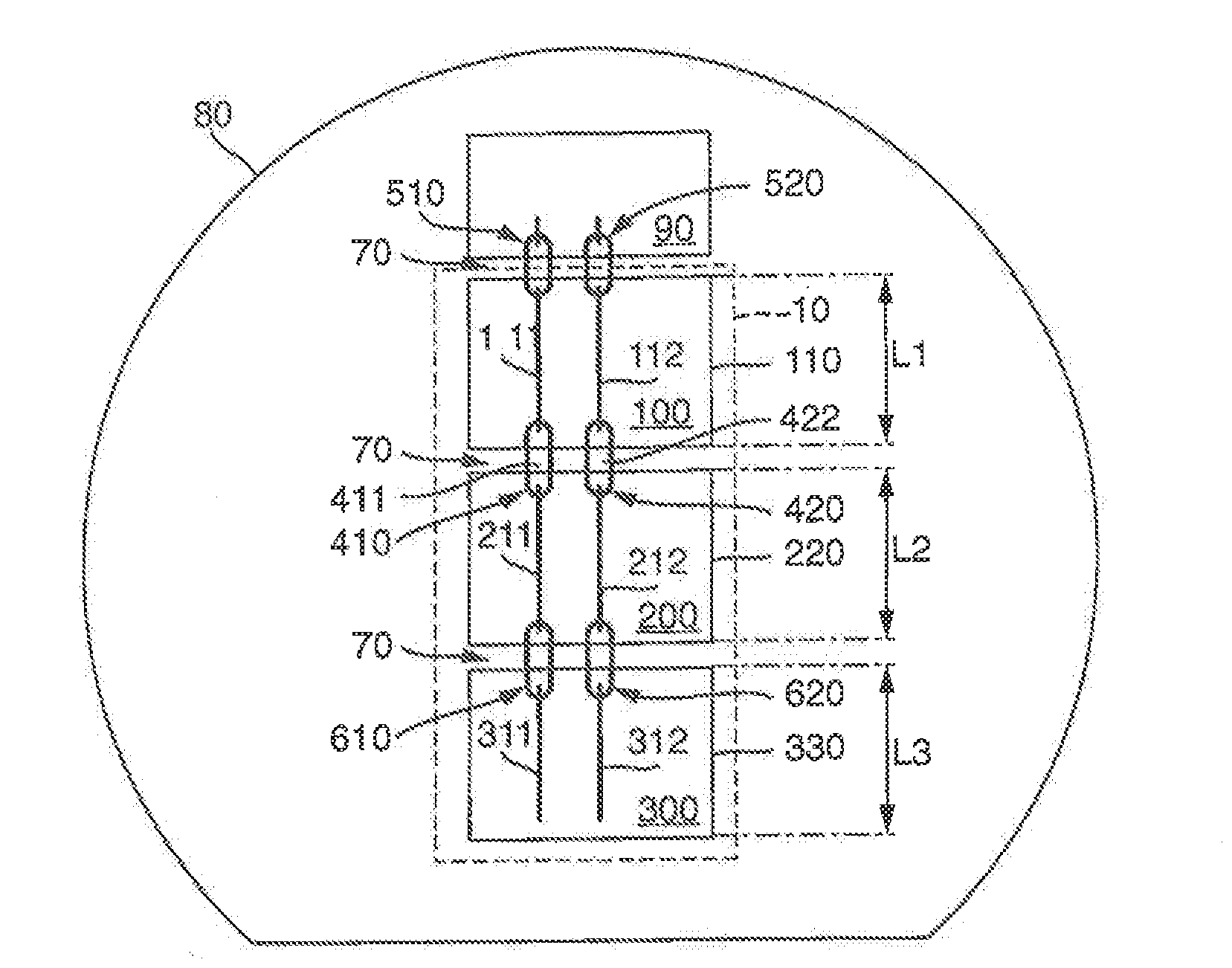
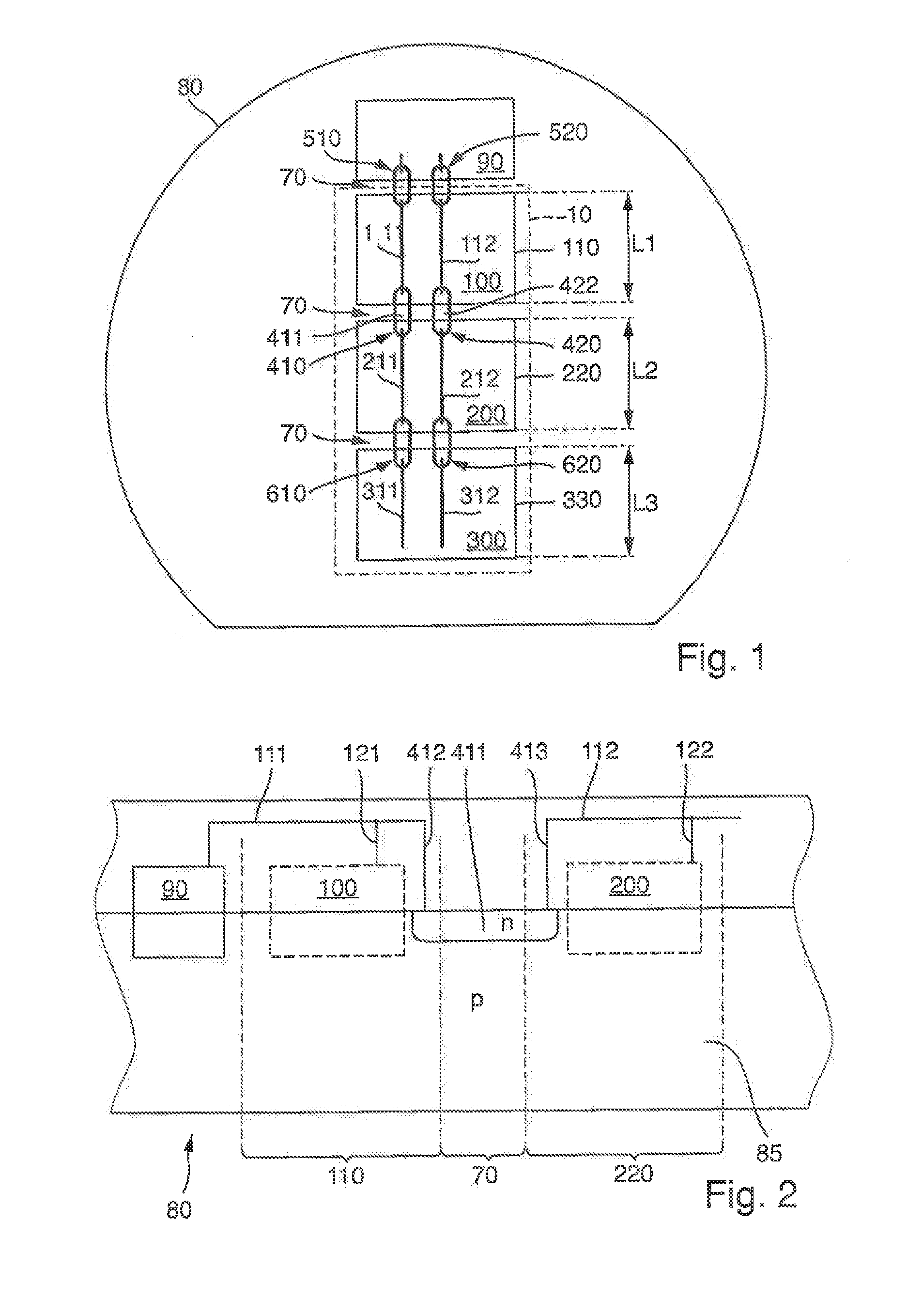
[0032]An arrangement for testing integrated circuits 100, 200, 300 is illustrated schematically in FIG. 1. Integrated circuits 100, 200, 300 are provided in a wafer 80 and have not yet been separated. FIG. 1 also shows an integrated test circuit 90. For the sake of simplicity, no terminal areas for connection to a separate test instrument are shown in FIG. 1. The greatly simplified view in FIG. 1 schematically shows electrical connections 111, 112, 211, 212, 311, 312, 410, 420, 510, 520, 610, 620, which, however, cannot be visible from the outside in the case of a finally processed wafer 80.

[0033]FIG. 1 shows a cluster 10 of integrated circuits 100, 200, 300 in wafer 80. Cluster 10 designates a group of integrated circuits 100, 200, 300 disposed adjacent to each other. Integrated circuits 100, 200, 300 usually have a plurality of components. All integrated circuits 100, 200, 300 of cluster 10 are provided in exactly one row or in exactly one column or in multiple rows and / or multipl...


PUM


Abstract

An arrangement for testing integrated circuits includes an integrated test circuit and a cluster which has at least one integrated circuit and a second integrated circuit. The first integrated circuit is provided in a first component region of a wafer, and the second integrated circuit in a second component region. The first component region and the second component region are spaced a distance apart by a scribe line of the wafer. The integrated test circuit is connected to the first integrated circuit via a first test line section, and the second integrated circuit is connected to the first test line section via a first connecting line that has a first well in the semiconductor material, the first well extending continuously in the wafer from the first component region over the scribe line to the second component region, the first well being electrically insulated from a substrate of the wafer.

Description

[0001]This nonprovisional application claims priority under 35 U.S.C. §119(a) to German Patent Application No. 10 2014 008 840.5, which was filed in Germany on Jun. 20, 2014, and which is herein incorporated by reference.BACKGROUND OF THE INVENTION[0002]1. Field of the Invention[0003]The present invention relates to an arrangement for testing integrated circuits provided in a wafer.[0004]2. Description of the Background Art[0005]A semiconductor wafer testing system is known from DE 103 42 312 A1, which corresponds to U.S. Pat. No. 6,888,365. Integrated circuits generally begin their manufacturing process in the form of a semiconductor die or integrated circuit, chip or “die” on a flat, circular wafer, which is called a substrate or semiconductor substrate. The semiconductor die usually comprises a rectangular part of the wafer surface and is also known under the designation of integrated circuit, chip, circuit or the like. Each wafer is usually segmented by scribe or saw lines into ...

Claims


Application Information

Patent Timeline
IPC IPC(8): G01R31/28
CPCG01R31/2884H01L22/34
Inventor RITTER, JOACHIM
Owner TDK MICRONAS GMBH
Learn More