Capacitor array and layout design method thereof

a technology of capacitor array and layout design, applied in the field of capacitor array, can solve the problems of system deterioration of mdac performance, and mdac may put up a bad performance or even come to adcs failure, so as to eliminate the error of capacitance mismatching

Active Publication Date: 2015-12-24
CHONGQING GIGACHIP TECH CO LTD
View PDF6 Cites 6 Cited by
  • Summary
  • Abstract
  • Description
  • Claims
  • Application Information

AI Technical Summary

Benefits of technology

[0012]It is an object of the invention to provide a layout design method to generate a matched unit capacitor array. The invention helps to eliminate capacitance mismatching error caused by parasitic capacitance in ways that generate a matched capacitor array. Featuring simplicity and small sized capacitor array, the invention can find applications in digital-to-analog converters requiring well-matched capacitor arrays and switched capacitance filters in general and high resolution pipelined ADC in particular.

Problems solved by technology

Otherwise it leads to gain errors deteriorating the performance of MDAC.
In a word, if each unit capacitor weights differently, the MDAC may put up a bad performance or even come to ADCs' failure.
The system error of capacitance mismatching is mainly caused by: (1) mismatched perimeter ratio caused by lithography process, (2) proximity effect in unit capacitor photolithography, (3) oxidation gradients and (4) mismatched parasitic capacitance.
A concentric layout features complexity and complicated wiring modes leading to increased inner and external lead parasitic capacitance, mismatching caused by parasitic capacitance and unnecessary chip size as capacitance matching types increases.
Different layouts and wiring modes of MDAC capacitor array have various parasitic capacitance of each unit capacitor which leads to different unit capacitance CA causing mismatched capacitance, gain errors of transfer function and DAC's error.
It has bad influence on the performance of MDAC and the linearity of ADC and even contributes to the failure of ADCs.
As MOS technology grows, the size of capacitors decreases and parasitic capacitance, being larger than unit capacitance, can no longer be ignored.
It is a challenge to design an MDAC capacitor array layout within a limited area eradicating mismatching error of capacitance caused by parasitic capacitance and generating a matched capacitor array.

Method used


Image

  • Capacitor array and layout design method thereof
  • Capacitor array and layout design method thereof
  • Capacitor array and layout design method thereof

Examples


Embodiment Construction

[0041]Hereinafter, the preferred embodiments of the present invention will be described with the accompanying drawings. It should be understood that the following embodiments are provided just for describing the invention, instead of limiting the property protection scope of the invention.

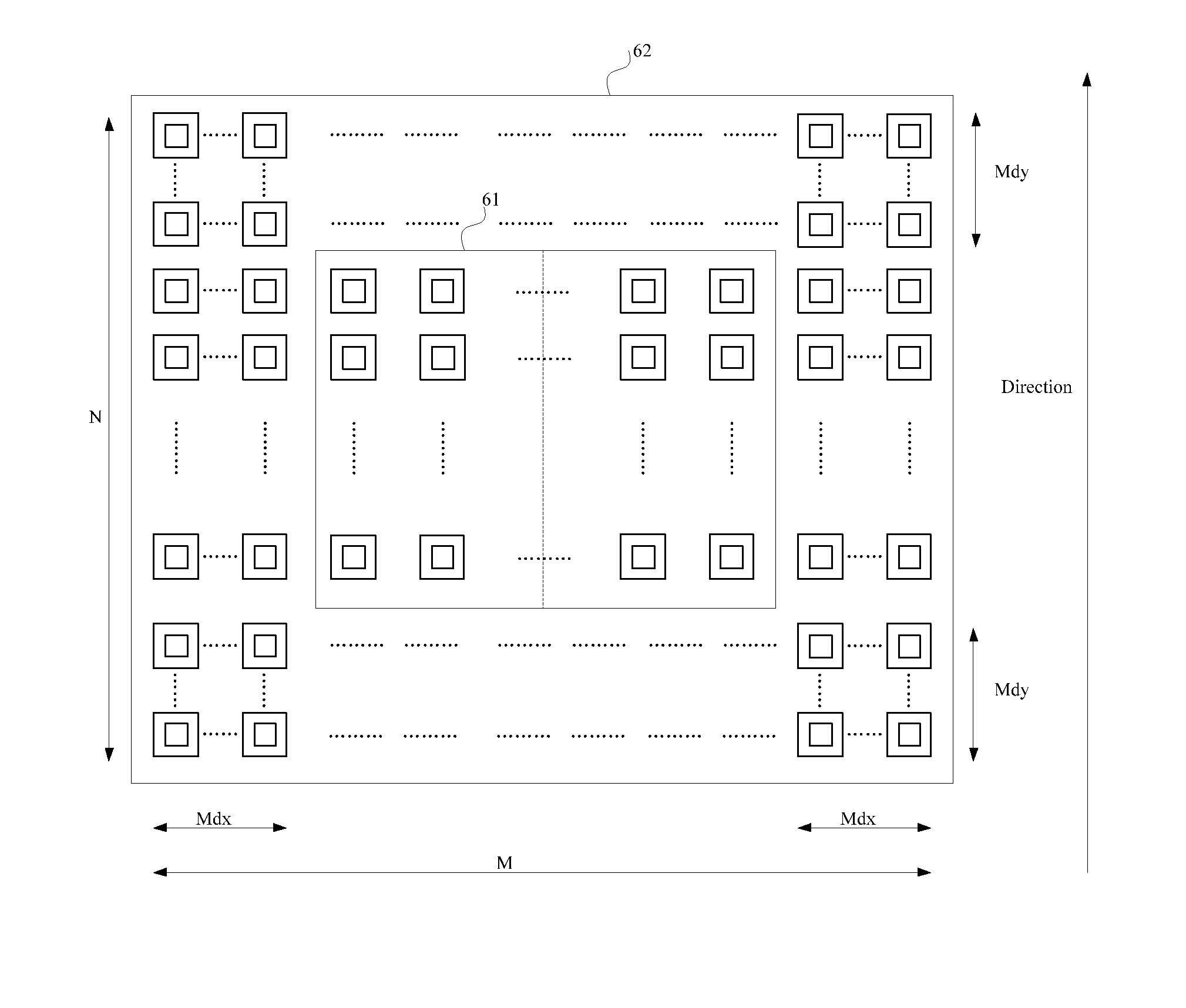
[0042]The MDAC capacitor array, featuring symmetric unilateral capacitor arrays, is generated by designing one side of symmetric unilateral capacitor arrays. One unilateral capacitor array of MDAC capacitor array is illustrated for the capacitor array layout design of pipelined ADC.

[0043]If M and N are respectively lines and rows of capacitor array layout as shown in FIG. 8, wherein M denotes the numbers of capacitors being at right angles to signal current and N denotes the number of capacitors being paralleled to signal current. M and N are integral multiples of 0.5. When M and N are odd multiples of 0.5, the half of the dummy capacitors on the edge is applied to the layout. FIG. 8 shows inner ca...


PUM


Abstract

A layout design method is provided for generating capacitor arrays being described in four steps: first, the wiring mode of unit capacitors is defined allowing the wire being connected to the upper plate to parallel that to the lower one, second, a capacitor array layout is designed with capacitors being distributed in Mh lines, Mh is the maximum of capacitors' lines, the line numbers of Class 1 to Class K capacitors are defined in the unilateral capacitor array, third, the wiring mode is set for capacitor array making sure the lengths of the wires to the upper and lower plates of unit capacitors are equal, at last, parasitic parameters are characterized in ways that verify the layout. A capacitor array is provided as well. By eliminating capacitance mismatching caused by parasitic capacitance, the method works to generate a well-matched capacitor array in an easy and efficient way.

Description

1. FIELD OF THE INVENTION[0001]The invention relates to a capacitor array and its layout design method.2. DESCRIPTION OF RELATED ART[0002]Because of high speed, high resolution, low power and small size, pipelined Analog to Digital Converters (ADCs) have wide application in wideband communication system and video image process. As shown in FIG. 1, the pipelined ADC's conversion circuit includes N stages of sub-stage conversion circuits 101A, 101B . . . 101N and a Flash ADC 102. An analog signal VIN, as an input signal, is converted into k(1) bit digital codes and residual difference analog voltage Vres1 through the first sub-stage 101A (Stage 1 as shown in FIG. 1). The residual difference analog voltage Vres1 is then sent to the second sub-stage 101B (stage 2 as shown in FIG. 1) and converted into k(2) bit digital codes and residual difference analog voltage Vres2. In the same way, the residual difference analog voltage Vres(N−1) is sent to the N sub-stage 101N (stage N as shown in ...

Claims


Application Information

Patent Timeline
Patent Type & Authority Applications(United States)
IPC IPC(8): G06F17/50H01G4/38
CPCH01G4/38G06F17/5072H03M1/164H03M1/442H01G15/00G06F30/394G06F30/392G06F30/00
Inventor WANG, YANWANG, YU-XINHU, GANG-YILI, TINGLIU, TAOCHEN, GUANG-BING
Owner CHONGQING GIGACHIP TECH CO LTD
Why Eureka
Try Eureka