

Surface emitting laser and optical coherence tomography using the surface emitting laser
a surface emitting laser and laser technology, applied in the direction of laser details, instruments, measurement devices, etc., can solve the problems of inability to form a proper light-intensity distribution, limited wavelength variable width, and unsatisfactory multi-mode oscillation, etc., to achieve a larger gain
- Summary
- Abstract
- Description
- Claims
- Application Information
AI Technical Summary
Benefits of technology
Problems solved by technology
Method used
Image

Examples
example 1
[0139]As EXAMPLE 1, VCSEL according to this example is described with reference to FIG. 7. FIG. 7 is a schematic cross-sectional view showing a layer structure of VCSEL according to this example.
[0140]The VCSEL according to this example is configured of a compound semiconductor based on GaAs, and is designed to perform wavelength sweeping around the center wavelength of 1060 nm.
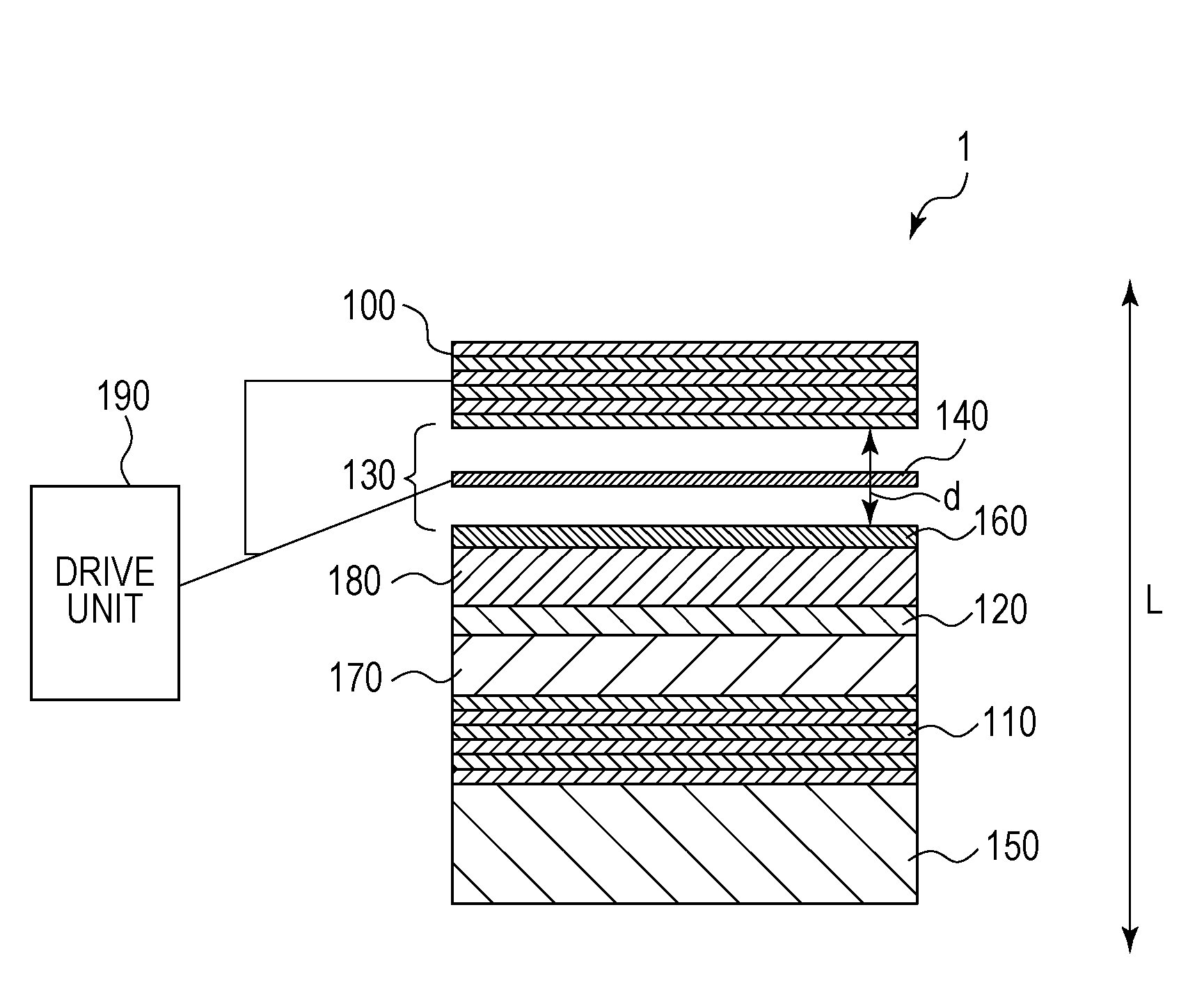
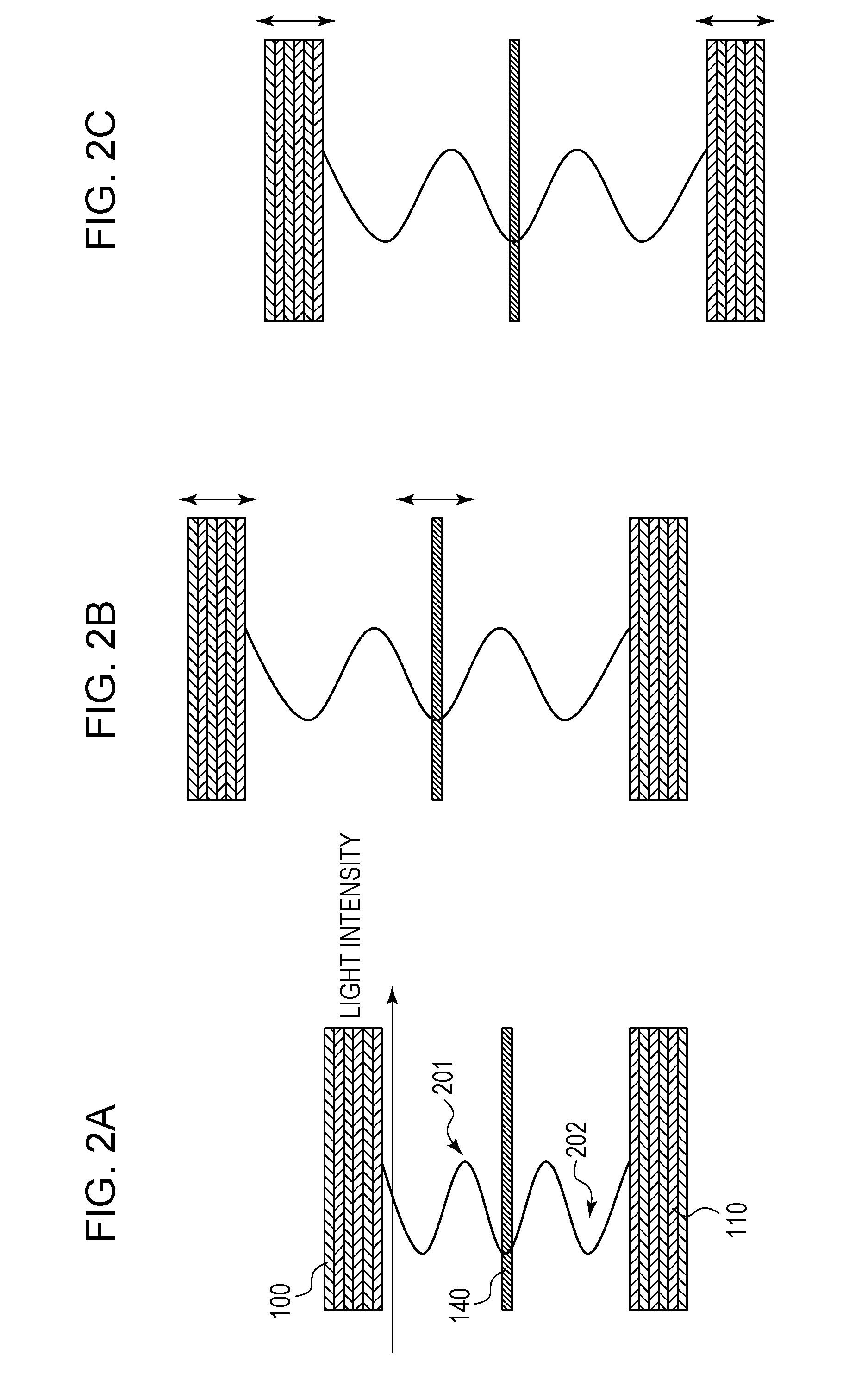
[0141]An upper reflecting mirror 700, an air gap 730, an antireflection film 760, an upper cladding layer 780, an active layer 720, a lower cladding layer 770, a lower reflecting mirror 710, and a GaAs substrate 750 are arranged in that order from the upper side. A light-intensity adjustment unit 740 is arranged in the air gap 730. The light-intensity adjustment unit 740 is configured of an Al0.7Ga0.3As layer with a thickness of 75 nm, and has an absorption coefficient of about 500 cm−1 by doping with an impurity.
[0142]The antireflection film 760 is formed of an oxidized AlAs layer with an optical thickness b...
example 2
[0159]FIG. 11 shows a schematic illustration explaining a configuration of a surface emitting laser according to EXAMPLE 2. In FIG. 11, an n-type multilayer-film mirror 1102 is provided on an n-type semiconductor substrate 1101 formed of a GaAs layer as a III-V group compound semiconductor. The n-type multilayer-film mirror (DBR) 1102 is a stack body in which 45 pairs of an Al0.8GaAs layer (68.1-nm-thick) and an Al0.3GaAs layer (62-nm-thick) as III-V group compound semiconductors are repetitively stacked.
[0160]On the multilayer-film mirror (DBR) 1102, an n-type cladding layer 1103 formed of an Al0.8GaAs layer (102.6-nm-thick) is provided. On the n-type cladding layer 1103, an active layer 1104 having a triple quantum well structure formed of a combination of a GaAs well layer (10-nm-thick) and an Al0.3GaAs barrier layer (10-nm-thick) is provided. Also, on the active layer 1104, a p-type cladding layer 1105 formed of an Al0.8GaAs layer (337.4-nm-thick) is further provided.
[0161]A mov...
example 3
[0175]A surface emitting laser according to EXAMPLE 3 is described with reference to FIG. 12. FIG. 12 is a schematic cross-sectional view showing a layer structure of VCSEL according to this example.
[0176]VCSEL 1200 according to this example includes a cathode electrode 1201 for driving VCSEL, an n-type substrate 1202 configured of GaAs, an n-type lower DBR 1203 formed by alternately stacking AlAs and GaAs by 40.5 pairs, an n-type lower spacer layer 1204 configured of Al0.7Ga0.3As, an undoped active layer 1205 configured of a multilayer quantum well layer formed of a quantum well layer of InGaAs and a barrier layer of GaAsP, and a p-type upper spacer layer 1206 configured of Al0.7Ga0.3As in that order. Also, an electrode 1207 for driving VCSEL and for driving upper DBR is formed on the upper spacer layer 1206. Further, an undoped GaAs layer 1208, an n-type slab portion 1209 configured of Al0.7Ga0.3As, an undoped GaAs layer 1210, an n-type upper DBR 1211 formed by arranging Al0.7Ga0....
PUM
 Abstract
Description
Claims
Application Information