

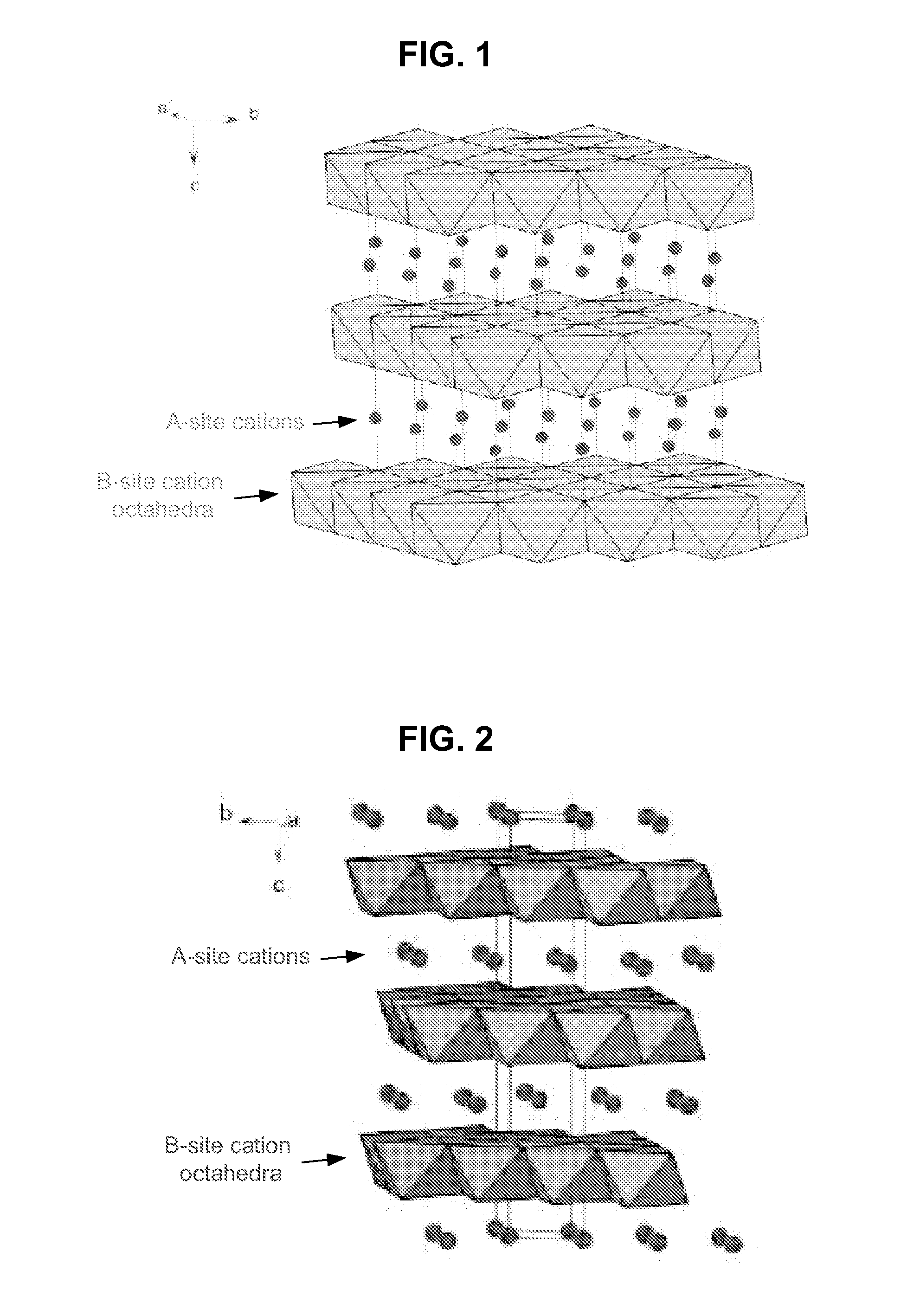
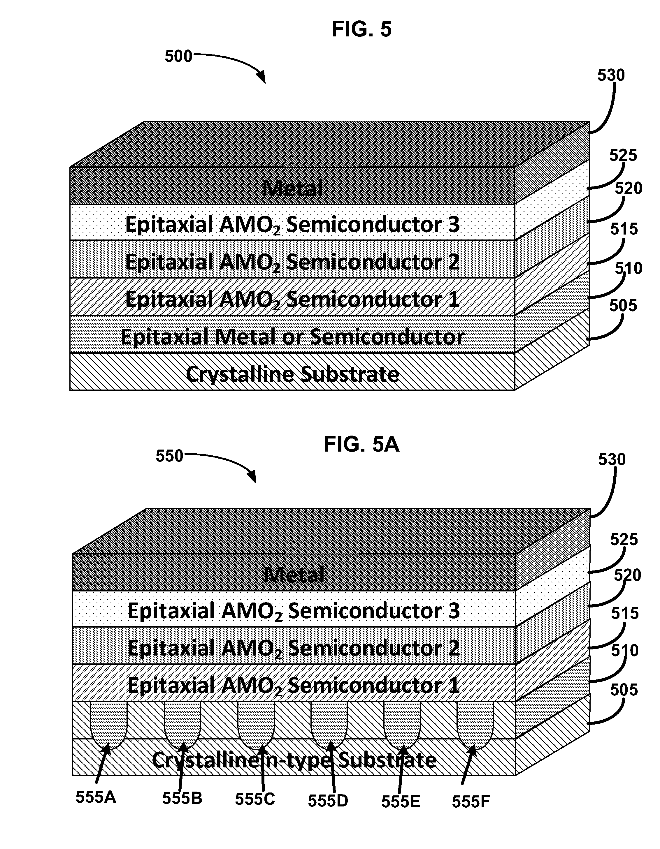
Lithium niobite compositions, syntheses, devices, and structures
a technology of lithium niobite and composition, applied in the field of semiconductor materials, can solve the problems of many impractical use, limitation of such materials, and difficulty in fabricating oxide semiconductors of p-typ
- Summary
- Abstract
- Description
- Claims
- Application Information
AI Technical Summary
Benefits of technology
Problems solved by technology
Method used
Image

Examples
examples
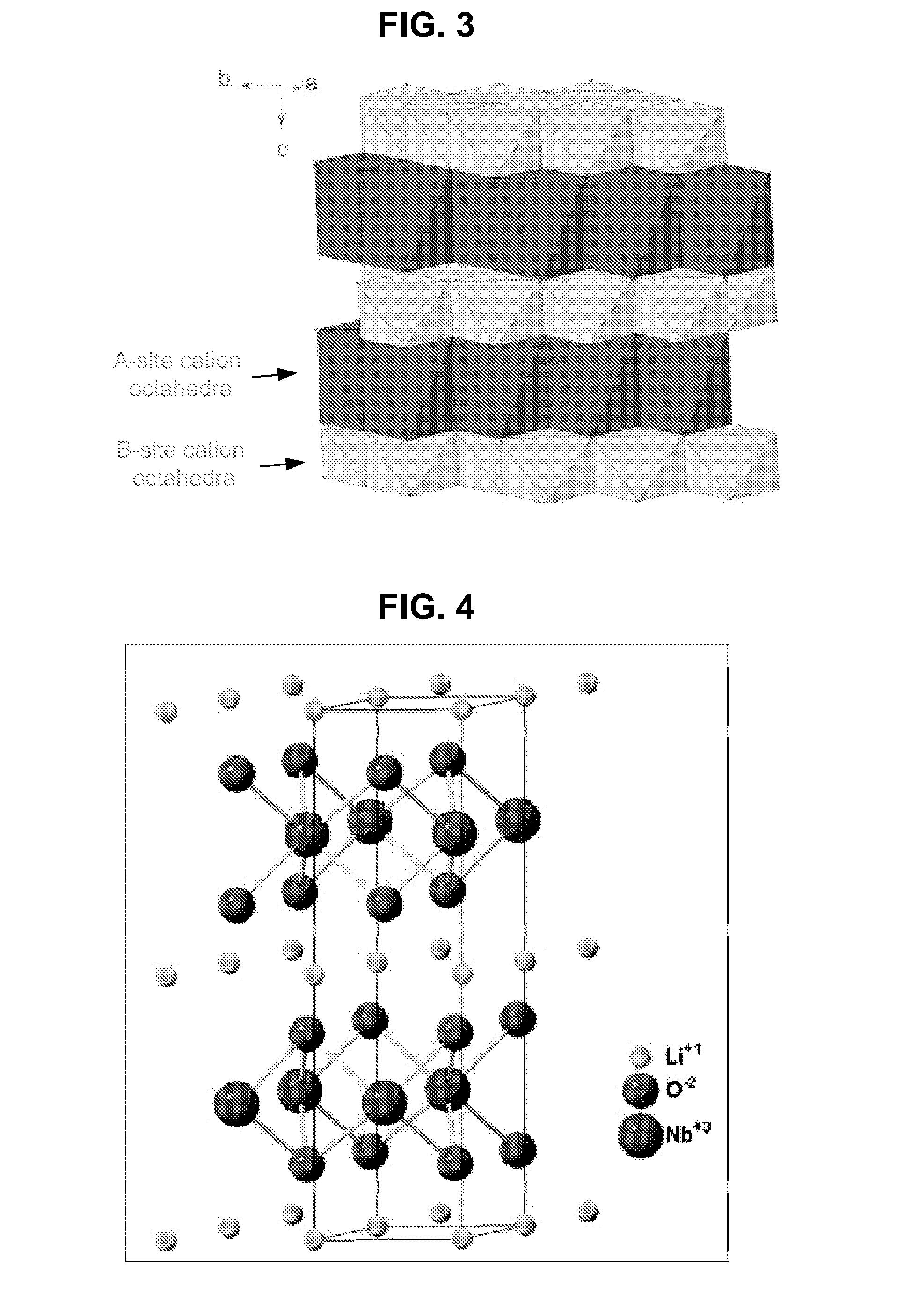
[0167]Crystal Growth of High Purity LiNbO2
[0168]LiNbO2 crystals were grown using an electrolytic reduction method in a LiBO2 (99.9%) flux. The flux allows Nb2O5, which has a high melting point of 1530° C., to become molten at readily achievable growth temperatures below 1000° C. Compared to previously used flux constituents, the LPEE-based growth method presented herein include only Nb2O5 (99.9%) and LiBO2 (99.9%), a marked change from previous methods used to grow crystalline LiNbO2, which include both NaBO2 and LiF as part of the growth constituent makeup. The molar ratio of LiBO2 to Nb2O5 used was 15:1 and is similar to the chemistry used in the growth of LiTiO2 (see Campá, J. A.; Vélez, M.; Cascales, C.; Gutiérrez Puebla, E.; Monge, M. A.; Rasines, I.; Ruíz-Valero, C. Journal of Crystal Growth 1994, 142 (1-2), 87-92.)
[0169]A nitrogen glove box environment was used throughout the growth of LiNbO2 crystals, and the humidity and temperature of the glove box were measured using an ...
PUM
| Property | Measurement | Unit |
|---|---|---|
| p-type conductivity | aaaaa | aaaaa |
| p-type conductivity | aaaaa | aaaaa |
| n-type conductivity | aaaaa | aaaaa |
Abstract
Description
Claims
Application Information