

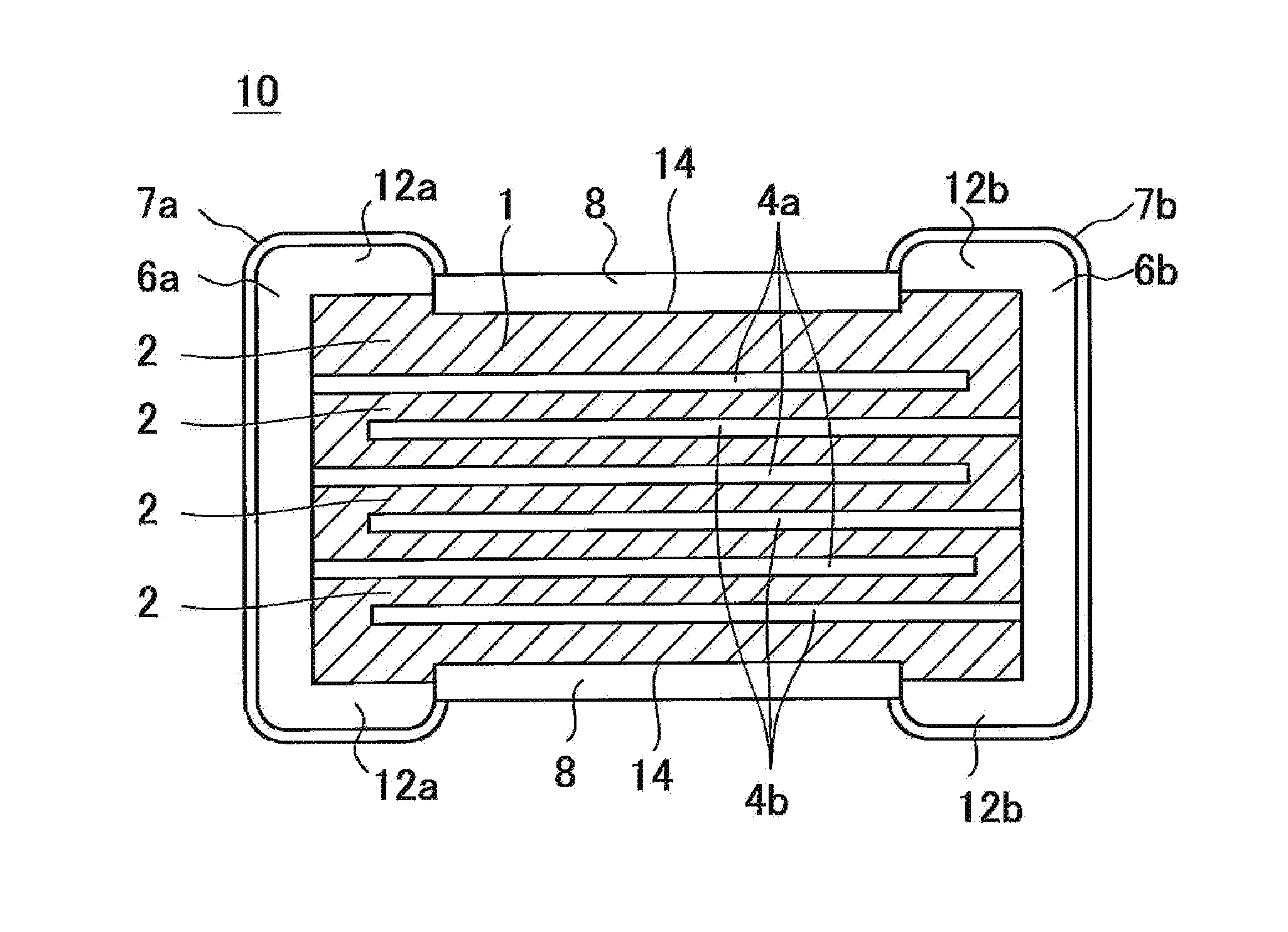
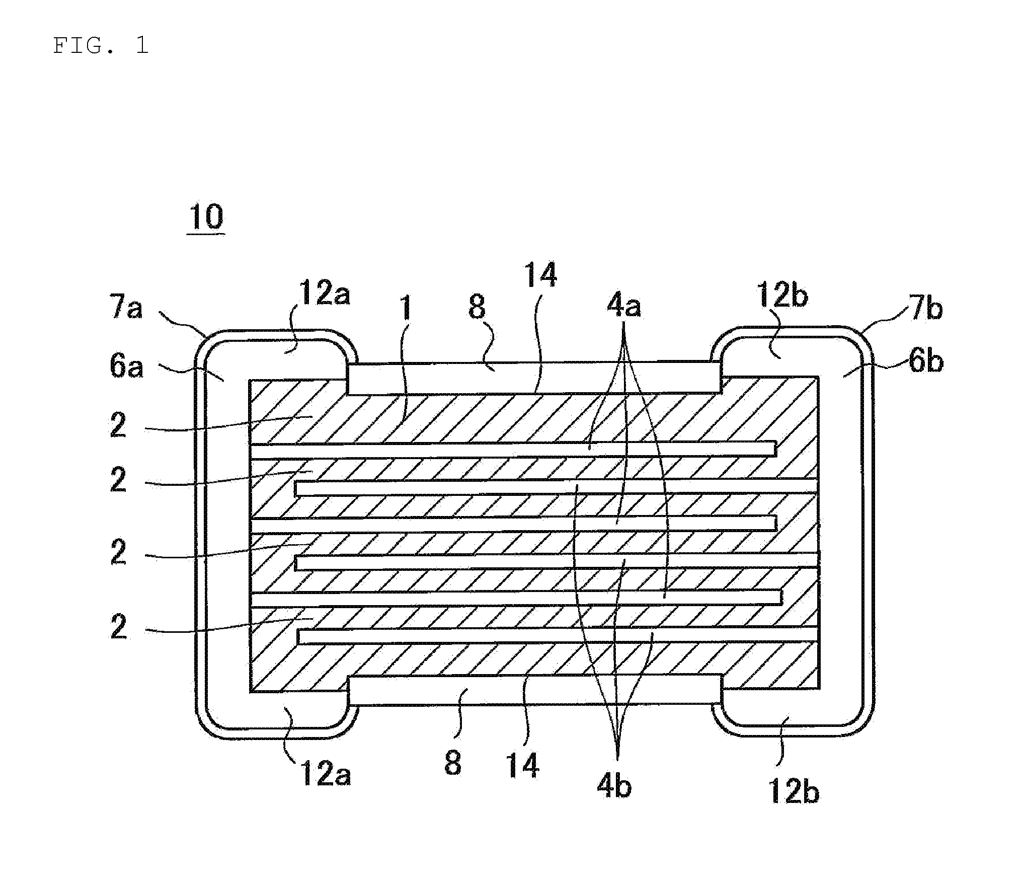
Ceramic electronic component
a technology of electronic components and ceramics, applied in the direction of fixed capacitor details, stacked capacitors, fixed capacitors, etc., can solve the problems of high manufacturing cost, high manufacturing cost, and inability to selectively achieve film formation, so as to improve chemical erosion resistance, high heat resistance, and manufacturing cost low cost
- Summary
- Abstract
- Description
- Claims
- Application Information
AI Technical Summary
Benefits of technology
Problems solved by technology
Method used
Image

Examples
example
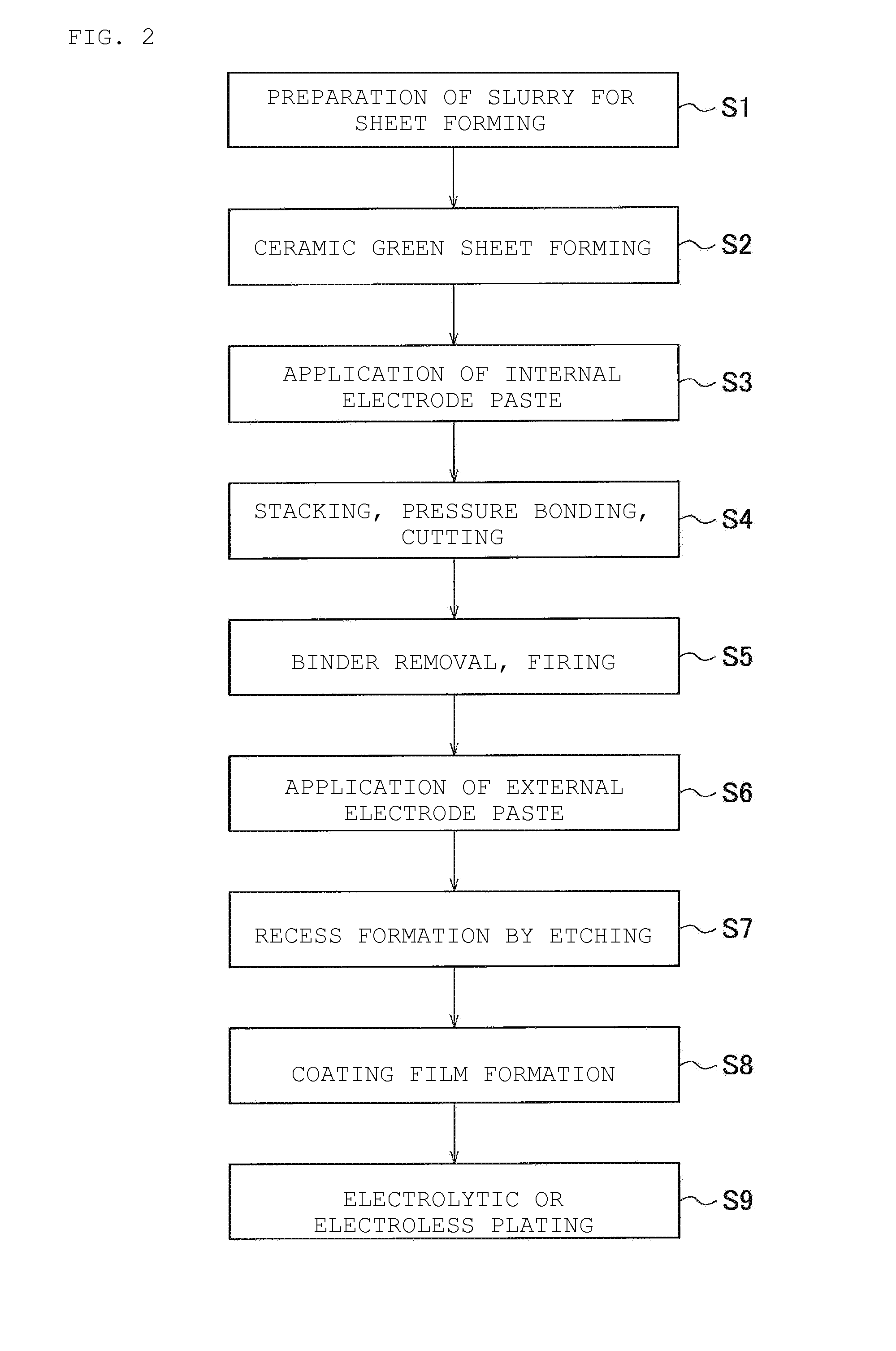
1. Preparation of Example and Comparative Example
[0066]The varistor 10 (with the recesses 14) according to an example and a varistor (without any recesses) according to a comparative example were each prepared by the manufacturing method according to the embodiment described previously. However, the immersion of the ceramic element in the etching solution in the step S7 was skipped in the case of the varistor according to the comparative example.
[0067]As the resin-containing solution, a commercially available latex of a resin component dispersed in an aqueous solvent was used with an etching promoting constituent and a surfactant added thereto, if necessary.
[0068]As the resin-containing solution, an acrylic resin (Trade Name: Nipol LX814A (from Zeon Corporation)) as the resin component was used through the adjustment of the pH to 4.0 with the addition of a sulfuric acid as the etching promoting constituent to the resin. To this resin, 1 vol % of NEWREX (registered trademark, from NO...
PUM
| Property | Measurement | Unit |
|---|---|---|
| Temperature | aaaaa | aaaaa |
| Thickness | aaaaa | aaaaa |
Abstract
Description
Claims
Application Information