Optoelectronic Control Of Solid-State Nanopores

a technology of optoelectronic control and nanopores, which is applied in the direction of material electrochemical variables, biochemical apparatus and processes, instruments, etc., can solve the problems of low current throughput, low current throughput, and interruption of open pore current levels

Active Publication Date: 2016-02-04
TRUSTEES OF BOSTON UNIV
View PDF0 Cites 9 Cited by
  • Summary
  • Abstract
  • Description
  • Claims
  • Application Information

AI Technical Summary

Benefits of technology

[0019]According to another embodiment of the invention, a method is provided that includes contacting a liquid containing a biopolymer with a solid-state insulating membrane having disposed therein a nanopore with at le

Problems solved by technology

When the nanopore is of molecular dimensions, passage of molecules causes interruptions in the open pore current level.
There are numerous challenges to develop effective nanopore detection techniques.
Two of the most significant challenges facing nanopore-assisted genomic sequencing are that molecular passage across the nanopore is higher than desired, and current

Method used


Image

  • Optoelectronic Control Of Solid-State Nanopores
  • Optoelectronic Control Of Solid-State Nanopores
  • Optoelectronic Control Of Solid-State Nanopores

Examples


examples

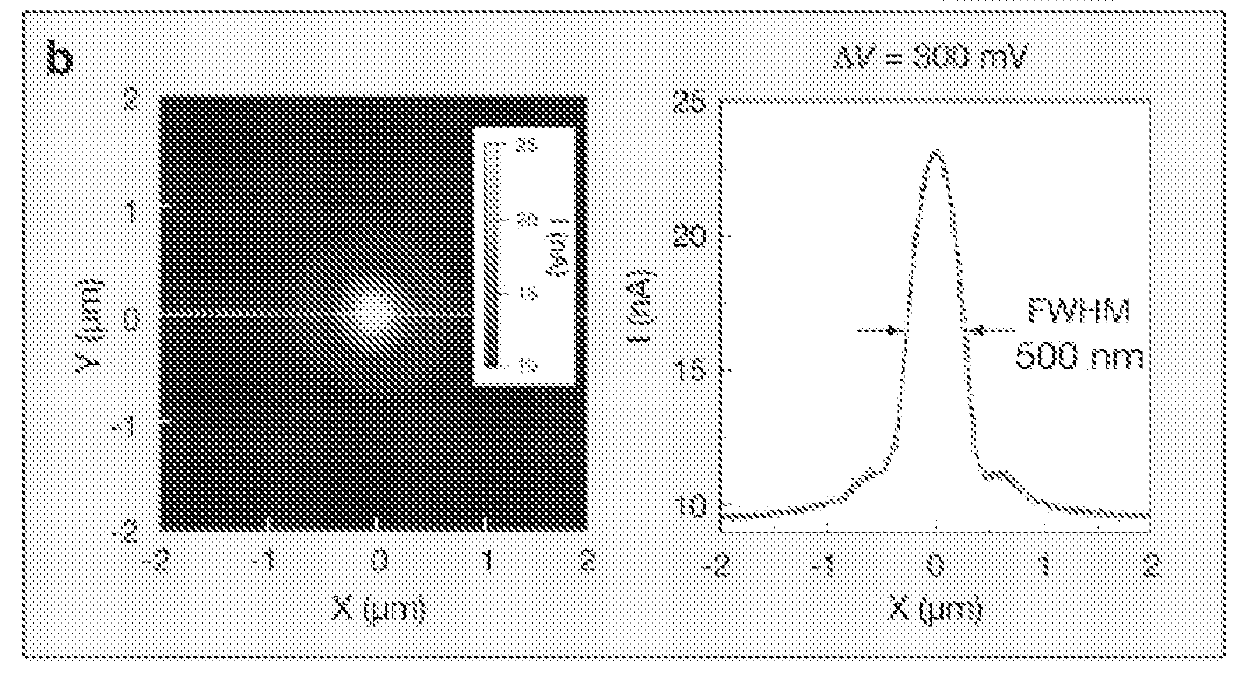
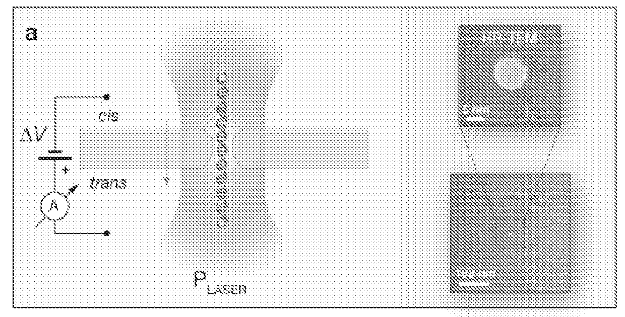
[0062]A high-resolution transmission electron microscope (TEM) was used to fabricate a single nanopore in silicon nitride membranes 30 nm thick. Piranha-cleaned chips were freshly assembled in a custom-made Teflon cell permitting low-noise electrical measurements and direct imaging using a high-magnification microscope objective (see Methods and FIG. 1a). A tightly-focused green laser (532 nm) in a custom-made confocal microscope illuminated the nanochip while a nanopositioner scanned a 4×4 μm2 area of the silicon nitride membrane. The ionic current (I) flowing through the pore at a fixed voltage level was continuously recorded during scanning.

[0063]Surprisingly, when the laser spot overlapped with the nanopore location there was an increase in I, with maximum magnitude more than twice that of the original current. This effect was evident even when using laser powers of just a few mW. This photo-conductance effect is illustrated in FIG. 1b: The upper panel shows TEM images of the 10...


PUM

PropertyMeasurementUnit
Fractionaaaaaaaaaa
Thicknessaaaaaaaaaa
Thicknessaaaaaaaaaa

Abstract

Optoelectronic control of solid-state nanopores and applications thereof. Nanopores are extremely sensitive single-molecule sensors. Electron beams have been used to fabricate synthetic nanopores in thin solid-state membranes with sub-nanometer resolution. Methods for controlling the translocation speed of biopolymers through solid-state nanopores and methods for unblocking clogged pores by illuminating nanopores are described.

Description

CROSS REFERENCE TO RELATED APPLICATION[0001]This application claims the benefit of U.S. Provisional Application No. 61 / 783,606, filed Mar. 14, 2013, the contents of which are hereby incorporated by reference.GOVERNMENT SUPPORT[0002]This invention was made with Government Support under Contract No. HG-005871 awarded by the National Institute of Health. The Government has certain rights in the invention.BACKGROUND[0003]1. Technical Field[0004]The present invention relates to optoelectronic control of solid-state nanopores and nanopore arrays, and applications thereof.[0005]2. Discussion of Related Art[0006]Nanopores, pores of nanometer dimensions in an electrically insulating membrane, have shown promise for use in a variety of sensing applications, including single molecule detectors. The nanopores used in such applications can be biological protein channels in a lipid bilayer or a pore in a solid-state membrane. Solid-state nanopores are generally made in silicon compound membranes,...

Claims


Application Information

Patent Timeline
IPC IPC(8): G01N21/63G01N33/487G01N27/49
CPCG01N33/48721G01N2201/06113G01N21/63G01N27/49C12Q1/6869C12Q2565/631
Inventor MELLER, AMITFIORI, NICOLAS DI
Owner TRUSTEES OF BOSTON UNIV
Why Eureka
Try Eureka