Optical fiber microwire devices and manufacture method thereof

Active Publication Date: 2016-02-04
JIANGSU UNIV
View PDF2 Cites 6 Cited by
  • Summary
  • Abstract
  • Description
  • Claims
  • Application Information

AI Technical Summary

Benefits of technology

[0005]This invention provide a new type of optical fiber microwires with the advantages of s

Problems solved by technology

Obviously, the small mode diameter leads to high nonlinearity.
However, simply reducing the diameter of the fiber core of a conventional optical fiber can not achieve small enough mode area.

Method used


Image

  • Optical fiber microwire devices and manufacture method thereof
  • Optical fiber microwire devices and manufacture method thereof
  • Optical fiber microwire devices and manufacture method thereof

Examples


embodiment 1

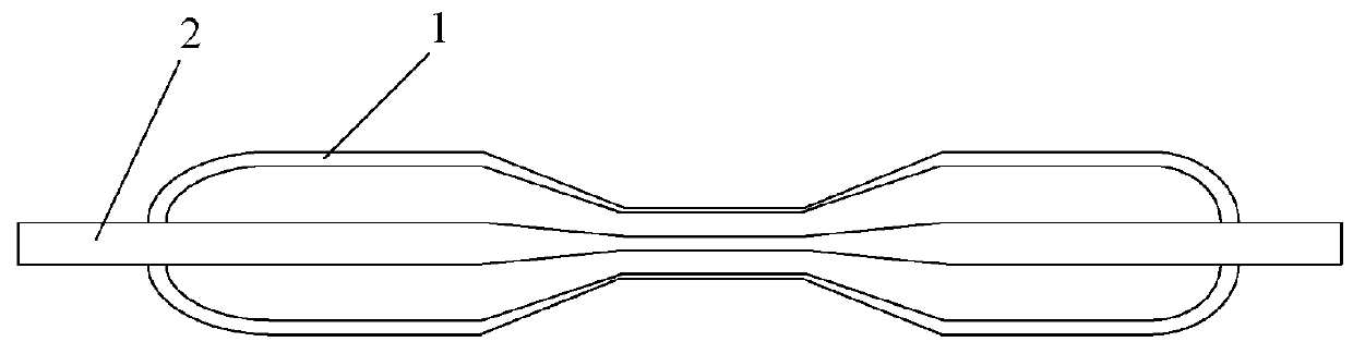
[0031]Single-mode optical fiber 2 with a cladding diameter of 80 μm, and a fiber length of 1 m is used. Optical fiber 2 is uncoated by 120 mm long in the middle segment. The length of silica tube 1 is 90 mm, the inner diameter is 900 μm and the thickness of silica tube 2 is 100 μm. The manufacture process follows the process 1. The optical fiber 2 need not be pre-tapered. The schematic diagram of the microwire device is shown in FIG. 1. The diameter and length of the waist of tapered optical fiber is 6.4 μm and 80 mm, respectively. The waist diameter of the silica tube 1 is 80 μm.

embodiment 2

[0032]Single-mode optical fiber 2 with a cladding diameter of 125 μm, and a fiber length of 1 m is used. Optical fiber 2 is uncoated by 50 mm long in the middle segment. The length of silica tube 1 is 65 mm, the inner diameter is 635 μm and the thickness of silica tube 1 is 265 μm. The manufacture process follows the process 1. The optical fiber need not be pre-tapered. The schematic diagram of the microwire device is shown in FIG. 1. The diameter and length of the waist of tapered optical fiber is 1.25 μm and 40 mm, respectively. The waist diameter of the silica tube 1 is 112 μm.

embodiment 3

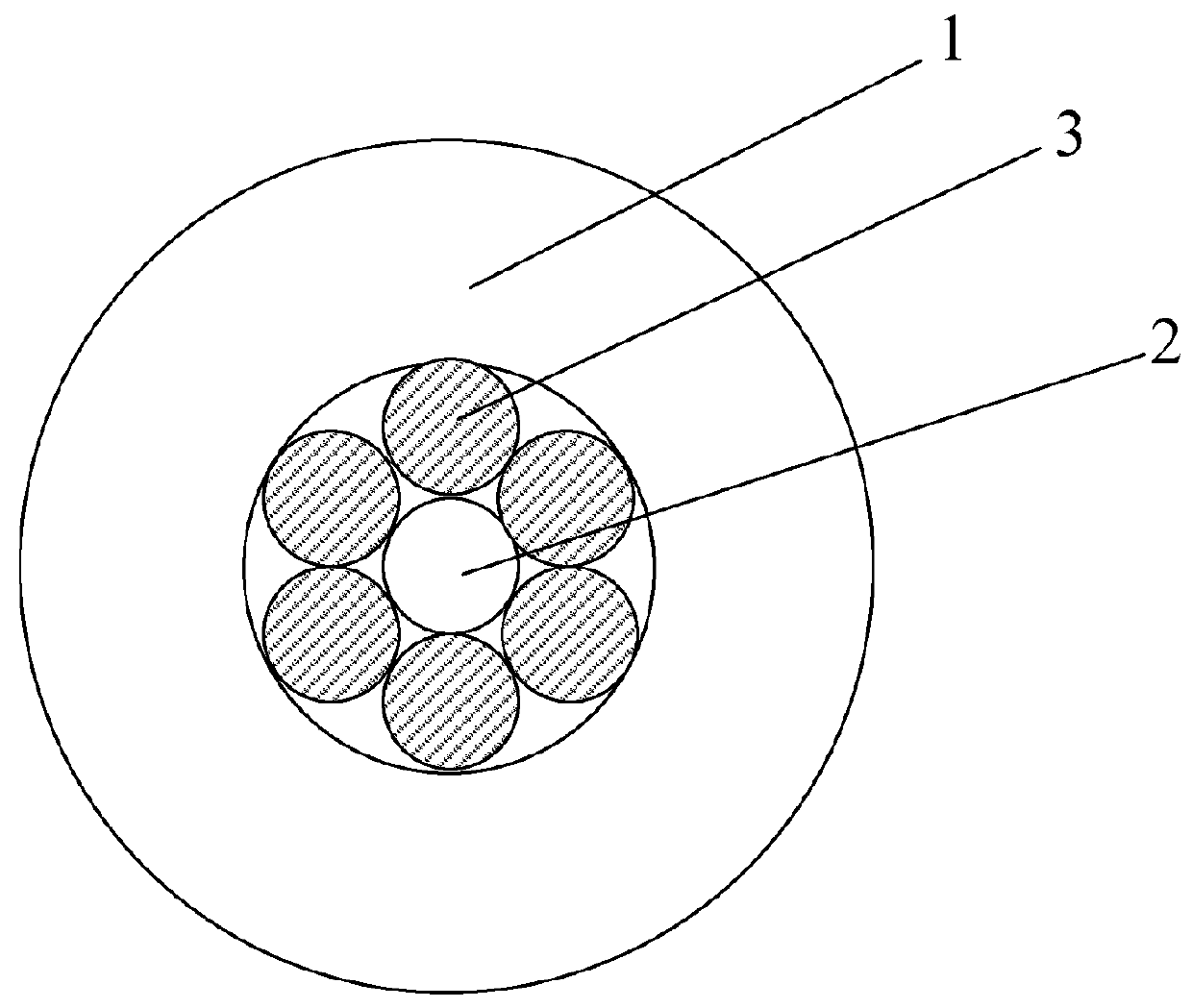
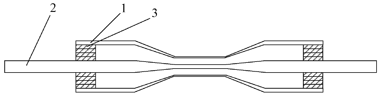
[0033]Single-mode optical fiber 2 with a cladding diameter of 125 μm, and a fiber length of 2 m is used. Optical fiber 2 is uncoated by 60 mm long in the middle segment. Pre-tapering is used to the optical fiber to form a waist diameter of 12 μm, and length of 50 mm. The length of silica tube 1 is 100 mm, and the inner diameter is 380 μm and the thickness of silica tube is 120 μm. The manufacture process follows the process 2. The silica tube 1 is filled with silica rods 3 at the two ends, the cross-section of the silica tube end is shown in FIG. 4. The schematic diagram of the microwire device is shown in FIG. 3. The diameter and length of the waist of tapered optical fiber is 2.4 μm and 60 mm, respectively. The waist diameter of the silica tube 1 is 100 μm.


PUM

PropertyMeasurementUnit
Lengthaaaaaaaaaa
Lengthaaaaaaaaaa
Thicknessaaaaaaaaaa

Abstract

Herein presents an optical fiber microwire device, wherein the device comprising a silica tube, an optical fiber (2) inserted into the silica tube (1) and pigtailed at two sides, wherein the two ends of the silica tube (1) are fused with the optical fiber (2) to form a solid structure, or the two ends of the silica tube (2) are filled with silica rods (3), silica capillaries (4) or segments of optical fibers and fused to form a solid structure. The silica tube (1) together with the optical fiber (2) inside is then tapered to form a micro structure region. Therefore, the micro structure region is consisted of the tapered optical fiber as the microstructure core, tapered silica tube, and the air in between. This invention combine the manufacture of optical fiber microwire and the sealing process, avoiding the disadvantages of the conventional tapered optical fiber microwire, such as fragile mechanical structure, and sensitive to the outer environment variations.

Description

TECHNICAL FIELD[0001]This invention relates to nonlinear optical fiber, in particular high nonlinear optical fiber microwire device.BACKGROUND OF THE PRESENT INVENTION[0002]Optical fiber microwire devices are well known for their advantages such as strong confinement, large evanescent fields, great configurability, low-loss connection, controllable dispersion, etc. According to the nonlinear coefficientγ=2πλn2π(ω2 / 4),wherein λ is the wavelength, ω is the mode field diameter, and n2 is the nonlinear-index coefficient. Obviously, the small mode diameter leads to high nonlinearity. However, simply reducing the diameter of the fiber core of a conventional optical fiber can not achieve small enough mode area. This is owing to the fact that the confinement ability of the fiber cladding with the reduction of core diameter. Increasing the index contrast between the core and the cladding is an efficient way to confine the core modes in a small core. Optical fiber nanowires and microwires can...

Claims


Application Information

Patent Timeline
IPC IPC(8): G02B6/02C03B37/15G02B6/032
CPCG02B6/02295C03B2203/14C03B37/15G02B6/032G02B6/107G02B6/2552G02B6/264G02B6/385
Inventor CHEN, MINGYANG
Owner JIANGSU UNIV
Why Eureka
Try Eureka