Organic photoelectronic device and image sensor and electronic device

an image sensor and electronic device technology, applied in the direction of thermoelectric device junction materials, semiconductor devices, electrical equipment, etc., can solve the problems of deterioration of sensitivity of silicon photodiodes and relatively small absorption area, so as to improve light absorption characteristics and wavelength selectivity. , the effect of increasing the wavelength selectivity

Active Publication Date: 2016-02-11
SAMSUNG ELECTRONICS CO LTD
View PDF0 Cites 9 Cited by
  • Summary
  • Abstract
  • Description
  • Claims
  • Application Information

AI Technical Summary

Benefits of technology

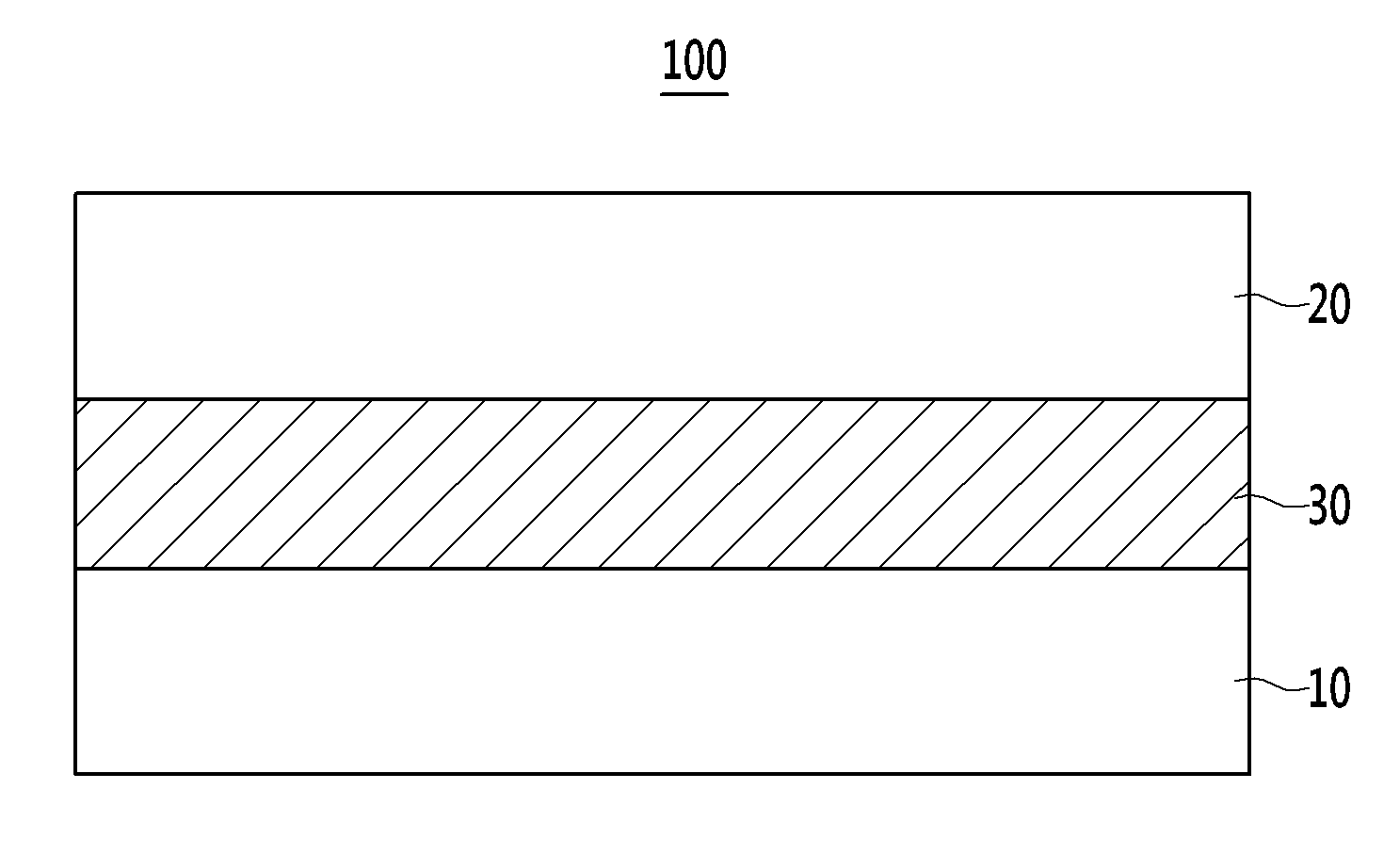
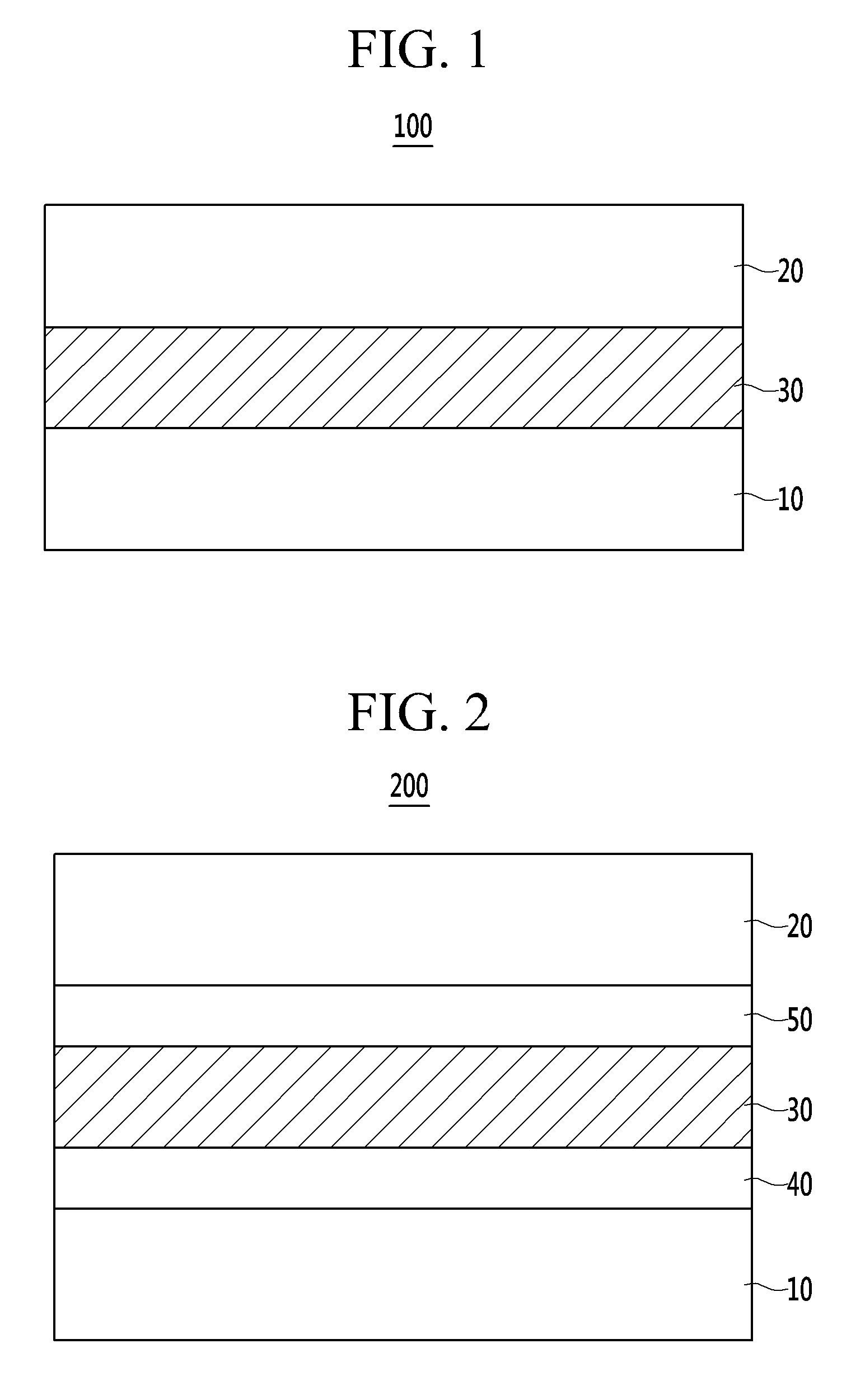
[0008]Example embodiments provide an organic photoelectronic device being capable of increasing wavelength selectivity by improving light absorption characteristics in a thin film state.

Problems solved by technology

At present, a silicon photodiode is widely used, but the silicon photodiode has a problem of deteriorated sensitivity and has a relatively small absorption area due to relatively small pixels.

Method used


Image

  • Organic photoelectronic device and image sensor and electronic device
  • Organic photoelectronic device and image sensor and electronic device
  • Organic photoelectronic device and image sensor and electronic device

Examples


synthesis example 1

[0146]

[0147]10.0 g of boron subphthalocyanine chloride (Aldrich) and 21.3 g of pentafluorophenol (Aldrich Corporation) are heated and refluxed in 150 ml of dry toluene for 15 hours. Subsequently, the reaction solution is concentrated under a reduced pressure and purified using silica gel column chromatography to obtain the compound represented by the Chemical Formula A.

synthesis example 2

[0148]

[0149]The compound represented by the Chemical Formula B is synthesized according to the same method as Synthesis Example 1, except that 6.6 g of 1-naphthol (Aldrich Corporation) is used instead of pentafluorophenol.

synthesis example 3

[0150]

[0151]The compound represented by the Chemical Formula C is synthesized according to the same method as Synthesis Example 1, except that 6.6 g of 2-naphthol (Aldrich Corporation) is used instead of pentafluorophenol.


PUM


Abstract

An organic photoelectronic device includes a first electrode and a second electrode facing each other, and an active layer between the first electrode and the second electrode and including a first compound represented by Chemical Formula 1 or 2, and a ratio between a FWHM of a light absorption curve depending on a wavelength of the first compound in a solution state and in a thin film state satisfies the following Relationship Equation 1: FWHM2 / FWHM1<2.5. In the Relationship Equation 1, FWHM1 is a FWHM of the light absorption curve depending on a wavelength in a solution state, and FWHM2 is a FWHM of the light absorption curve depending on a wavelength in a thin film state.

Description

CROSS REFERENCE TO RELATED APPLICATION[0001]This application claims priority to and the benefit of Korean Patent Application No. 10-2014-0101908 filed in the Korean Intellectual Property Office on Aug. 7, 2014, the entire contents of which are incorporated herein by reference.BACKGROUND[0002]1. Field[0003]Example embodiments relate to an organic photoelectronic device, an image sensor, and an electronic device.[0004]2. Description of the Related Art[0005]A photoelectronic device converts light into an electrical signal using photoelectronic effects, and may include a photodiode and / or a phototransistor. The photoelectronic device may be applied to an image sensor, a solar cell and / or an organic light emitting diode.[0006]An image sensor including a photodiode requires relatively high resolution and thus a relatively small pixel. At present, a silicon photodiode is widely used, but the silicon photodiode has a problem of deteriorated sensitivity and has a relatively small absorption ...

Claims


Application Information

Patent Timeline
Patent Type & Authority Applications(United States)
IPC IPC(8): H01L51/00H01L27/30H01L51/44
CPCH01L51/008H01L27/307H01L51/442H10K39/32H10K85/211H10K85/311H10K85/322H10K30/30H10K30/82H10K2102/103
Inventor YAGI, TADAORIE, SAKURAILEE, KWANG HEELEEM, DONG-SEOKBULLIARD, XAVIERSATOH, RYUICHIPARK, KYUNG BAEYUN, SUNG YOUNGLEE, GAE HWANGJIN, YONG WANHEO, CHUL JOON
Owner SAMSUNG ELECTRONICS CO LTD
Why Eureka
Try Eureka