Semiconductor structures and fabrication methods thereof

a technology of semiconductors and semiconductor substrates, applied in the direction of semiconductor devices, electrical equipment, transistors, etc., can solve the problems of increasing the defect rate of cmos transistors formed on bulk silicon semiconductor substrates, increasing the defect rate of cmos transistors, and increasing the doping concentration of channel regions of existing finfets

Active Publication Date: 2016-03-03
SEMICON MFG INT (SHANGHAI) CORP
View PDF9 Cites 13 Cited by
  • Summary
  • Abstract
  • Description
  • Claims
  • Application Information

AI Technical Summary

Problems solved by technology

Thus, more defects may occur in CMOS transistors formed on a bulk silicon semiconductor substrate.
Further, certain related effects, such as short channel effects, channel punch through effects, or reduction of gate control ability effects, etc., may become more severe using the bulk silicon semiconductor substrate.
Further, the doping concentration of the channel reg

Method used


Image

  • Semiconductor structures and fabrication methods thereof
  • Semiconductor structures and fabrication methods thereof
  • Semiconductor structures and fabrication methods thereof

Examples


Embodiment Construction

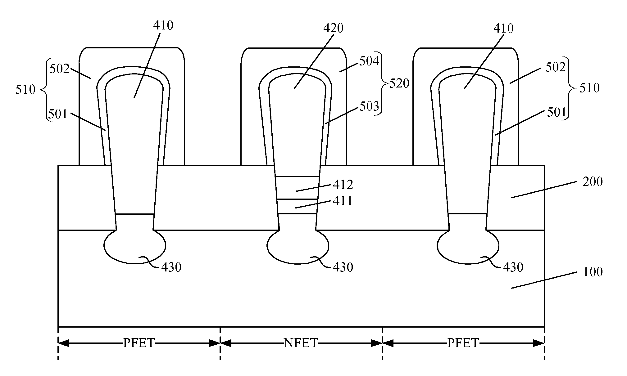
[0012]Reference will now be made in detail to exemplary embodiments of the invention, which are illustrated in the accompanying drawings. Wherever possible, the same reference numbers will be used throughout the drawings to refer to the same or like parts.

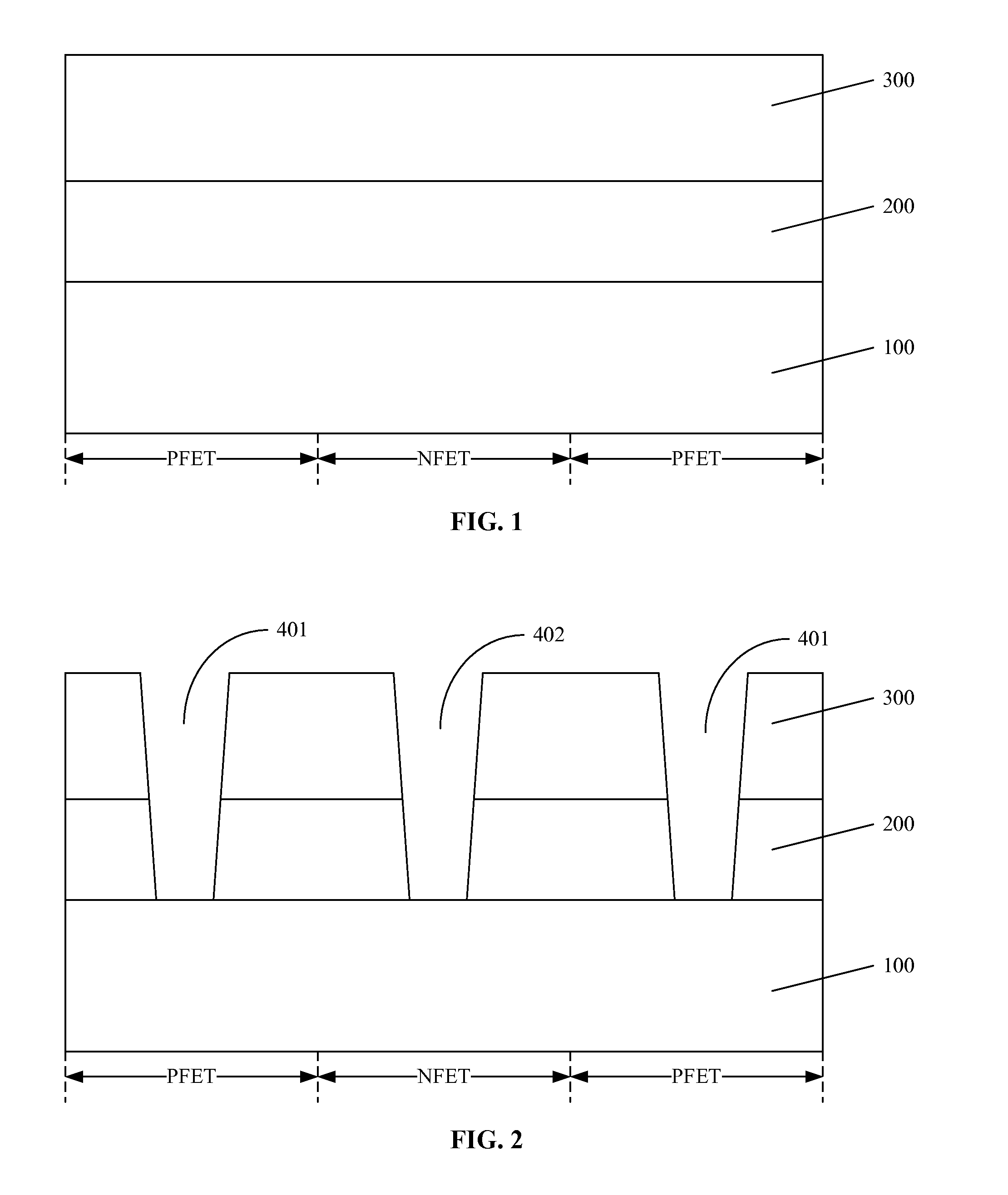
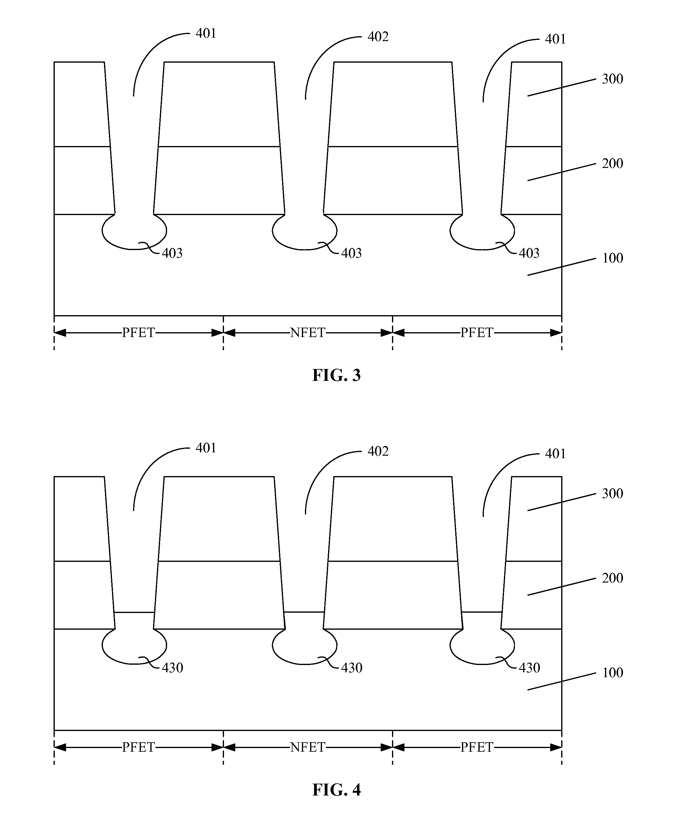
[0013]FIG. 12 illustrates an exemplary fabrication process of a semiconductor structure consistent with the disclosed embodiments; and FIG. 1˜11 illustrate semiconductor structures corresponding to certain stages of the exemplary fabrication process.

[0014]As shown in FIG. 12, at the beginning of fabrication process, a semiconductor substrate is provided (S101). FIG. 1 illustrates a corresponding semiconductor structure.

[0015]As shown in FIG. 1, a semiconductor substrate 100 is provided. The semiconductor substrate 100 may have a plurality of PFET regions and a plurality of NFET regions. For illustrative purposes, one NFET region and two PFET regions are shown in FIG. 1. Further, an insulation layer 200 may be formed on the surface ...


PUM


Abstract

A method for forming a semiconductor structure includes sequentially providing a semiconductor substrate having NFET regions and NFET regions; forming an insulation layer on the semiconductor substrate; forming a sacrificial layer on the insulation layer; forming first trenches in the PFET regions, and second trenches in in the NFET regions; forming a third trench on the bottom of each of the first trenches and the second trenches; forming a first buffer layer in each of the first trenches and the second trenches by filling the third trenches; forming a first semiconductor layer on each of the first buffer layers in the first trenches and the second teaches; removing the first semiconductor layers in the second trenches; forming a second buffer layer with a top surface lower than the insolation layer in each of second trenches; and forming a second semiconductor layer on each of the second buffer layers.

Description

CROSS-REFERENCES TO RELATED APPLICATIONS[0001]This application claims the priority of Chinese patent application No. 201410441272.5 filed on Sep. 1, 2014, the entirety of which is incorporated herein by reference.FIELD OF THE INVENTION[0002]The present invention generally relates to the field of semiconductor manufacturing technology and, more particularly, relates to semiconductor structures and fabrication processes thereof.BACKGROUND[0003]With the continuous development of semiconductor technology, the size of semiconductor devices has become smaller and smaller. Thus, more defects may occur in CMOS transistors formed on a bulk silicon semiconductor substrate. Further, certain related effects, such as short channel effects, channel punch through effects, or reduction of gate control ability effects, etc., may become more severe using the bulk silicon semiconductor substrate. In order to improve the performance of the semiconductor devices formed on the bulk silicon semiconductor ...

Claims


Application Information

Patent Timeline
IPC IPC(8): H01L21/8238H01L27/092
CPCH01L21/823821H01L27/0924H01L21/823814H01L21/823807H01L21/02532H01L21/02543H01L21/02546H01L21/02549H01L21/02576H01L21/02579H01L21/02636H01L21/3065H01L21/324H01L21/823878H01L21/8258H01L29/0649H01L29/0847H01L29/267H01L29/66636H01L29/7848
Inventor XIAO, DEYUAN
Owner SEMICON MFG INT (SHANGHAI) CORP
Why Eureka
Try Eureka