
Digital circuit design method and associated computer program product

a digital circuit and computer program technology, applied in the field of circuit design, can solve problems such as inability to check circuits with static timing analysis, difficulty in doing this kind of simulation, and product schedules that may be affected

Active Publication Date: 2016-03-17
REALTEK SEMICON CORP
View PDF1 Cites 6 Cited by
  • Summary
  • Abstract
  • Description
  • Claims
  • Application Information

AI Technical Summary

Benefits of technology

The present invention provides a method and computer program for designing digital circuits. The method involves performing pre-post-layout simulation before physical design to discover potential errors and constraints in the circuit design. This is achieved by performing logic synthesis, retrieving information of specific nodes, generating an updated standard delay format file with less delay, and using the netlist and updated standard delay format file for the pre-post-layout simulation. The technical effect of this invention is to improve the accuracy and efficiency of digital circuit design.

Problems solved by technology

In general, after the logic synthesis but before the physical design, the functional simulation with the timing delay information is not needed, besides doing this kind of simulation is difficult.
However, since the post-layout simulation, executed after the physical design, usually is pretty close to tape out, if the problems are discovered in post-layout simulation, the product schedule may be affected.
However, sometimes engineers make mistakes in designing the timing constraints so that the static timing analysis is performed with a timing-loosening constraint and that the errors can not be discovered until the post-layout simulation.
Some circuits even can not be checked with static timing analysis, in which case, with current design flow, the error can possibly be discovered only in the post-layout simulation.
However, as the abovementioned statements, it's usually too late if this kind of error is discovered after the physical design.

Method used


Image

  • Digital circuit design method and associated computer program product
  • Digital circuit design method and associated computer program product
  • Digital circuit design method and associated computer program product

Examples


Embodiment Construction

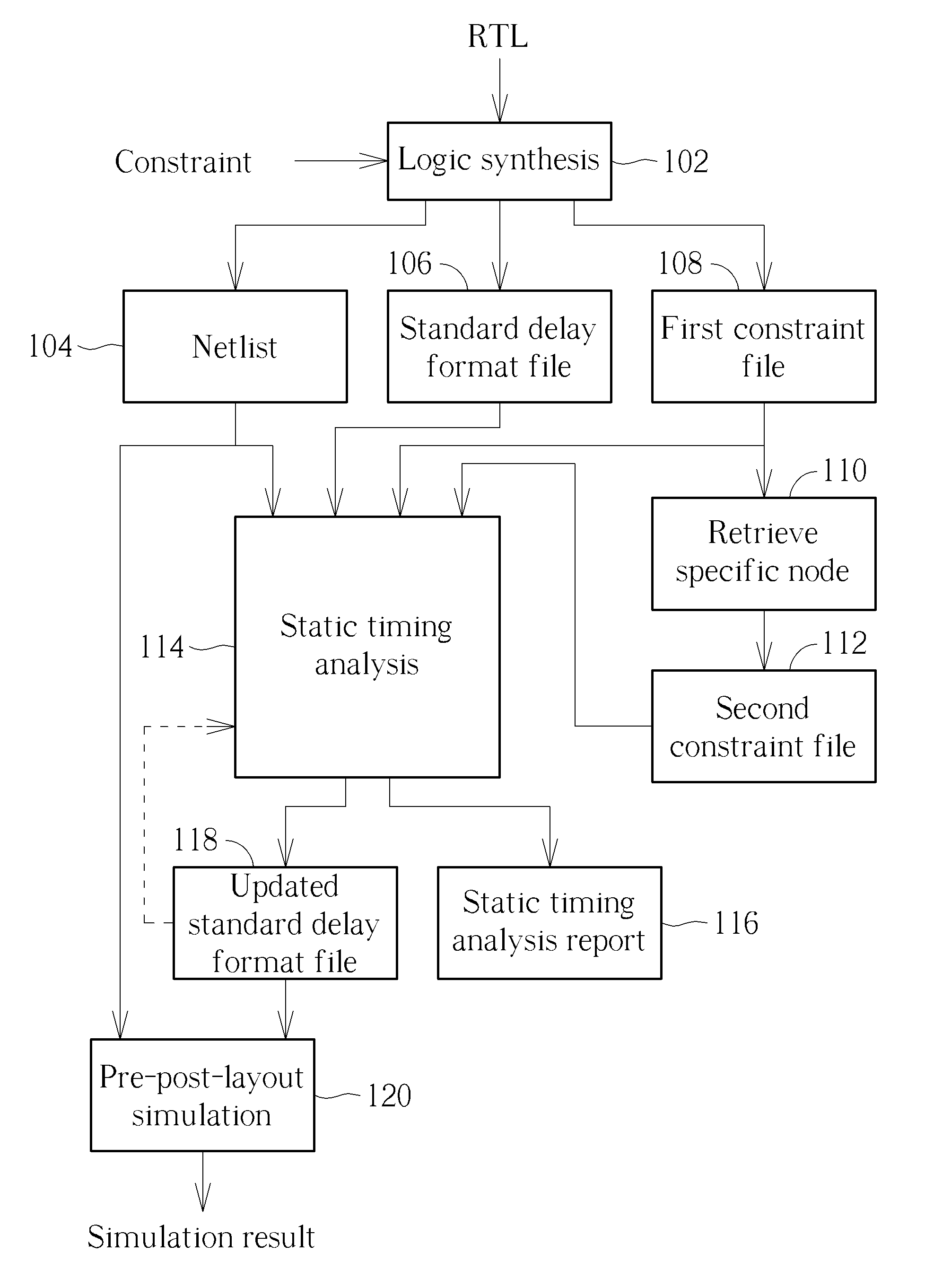
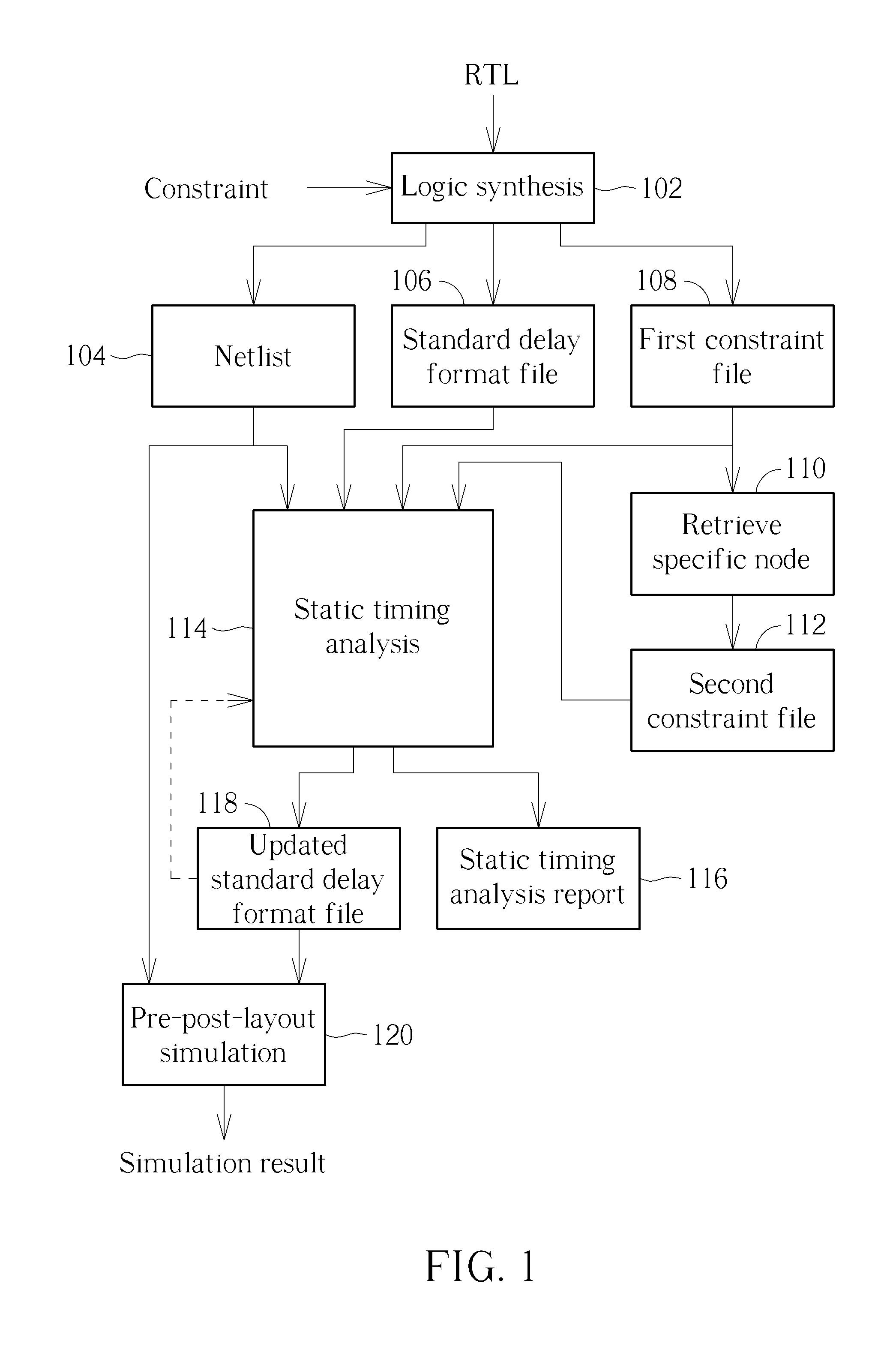
[0016]FIG. 1 is a flowchart illustrating a digital circuit design method according to an embodiment of the present invention. In this embodiment, the digital circuit design method is executed by a plurality of program instructions after a computer program product is loaded by a computer / processor. Refer to FIG. 1, the flow of the digital circuit design is described as follows.

[0017]First, in step 102, a logic synthesis operation is performed according an RTL design and a plurality of constraints to generate a netlist, a standard delay format (SDF) file and a first constraint file in steps 104, 106 and 108. The above constraints are designed by engineers, and mainly comprise contents such as pins on which clocks of certain frequencies are created for the synchronous digital circuit. The netlist is a kind of file format for describing circuit, which is logically equivalent to the RTL design, and satisfies the constraints given by engineers. The standard delay format file mainly descri...


PUM


Abstract

A digital circuit design method includes: before performing physical design: performing a logic synthesis according to a Register Transfer Level (RTL) design and a plurality of constraints to at least generate a netlist, a standard delay format file and a first constraint file; retrieving information of at least a specific node of circuit from the first constraint file to generate a second constraint file; generating an updated standard delay format file at least according to the standard delay format file and the second constraint file, wherein a delay of the specific node of the updated standard delay format file is less than a delay of the specific node of the standard delay format file; and using the netlist and the updated standard delay format file to perform a pre-post-layout simulation.

Description

BACKGROUND OF THE INVENTION[0001]1. Field of the Invention[0002]The present invention relates to a circuit design, and more particularly, to a digital circuit design method and associated computer program product.[0003]2. Description of the Prior Art[0004]Traditional digital circuit design is mainly categorized into front-end stage and back-end stage, wherein the front-end stage mainly comprises Register Transfer Level (RTL) design, functional simulation and logic synthesis, and the back-end stage comprises physical design, automatic placement and routing, and post-layout simulation, etc.[0005]In general, after the logic synthesis but before the physical design, the functional simulation with the timing delay information is not needed, besides doing this kind of simulation is difficult. For example, in the setting of the logic synthesis, high fan-out nets of the circuit will be annotated with huge delay times in the timing information generated by the logic synthesis, so the netlist...

Claims


Application Information

Patent Timeline
IPC IPC(8): G06F17/50
CPCG06F17/505G06F30/398G06F30/3312G06F30/327G06F2119/12G06F2111/04G06F30/3315
Inventor TSENG, SHUN-TEWENG, CHI-SHUN
Owner REALTEK SEMICON CORP
Learn More