Power semiconductor device and gate driver circuit

Inactive Publication Date: 2016-03-17
KK TOSHIBA
View PDF0 Cites 9 Cited by
  • Summary
  • Abstract
  • Description
  • Claims
  • Application Information

AI Technical Summary

Benefits of technology

The patent describes a power semiconductor device and a gate driver circuit that address issues related to voltage noise and malfunction caused by high side driver in a half-bridge gate driver circuit. The device includes a driving direct-current power supply and a pulse generating circuit that generate control signals for the gate driver circuit. The gate driver circuit includes an RS flip-flop circuit that receives a set pulse signal and a reset pulse signal and outputs a first control signal. The device also includes a latch circuit that receives the set and reset pulse signals and outputs a first reset signal obtained by masking out a pulse of the reset pulse signal during a period in which the set and reset pulse signals overlap with each other. The technical effect of the patent is to provide a more reliable and efficient power semiconductor device with improved control of the high side driver and reduced malfunctions caused by voltage noise.

Problems solved by technology

If the control signal turns on the high side switching element while the low side switching element is in the off state, for example, the potential at the output terminal of the half-bridge gate driver circuit changes from 0V to the power supply potential of the high side power supply, and a voltage noise occurs.
In this way, the voltage noise can cause malfunction of the high side driver.

Method used


Image

  • Power semiconductor device and gate driver circuit
  • Power semiconductor device and gate driver circuit
  • Power semiconductor device and gate driver circuit

Examples


first embodiment

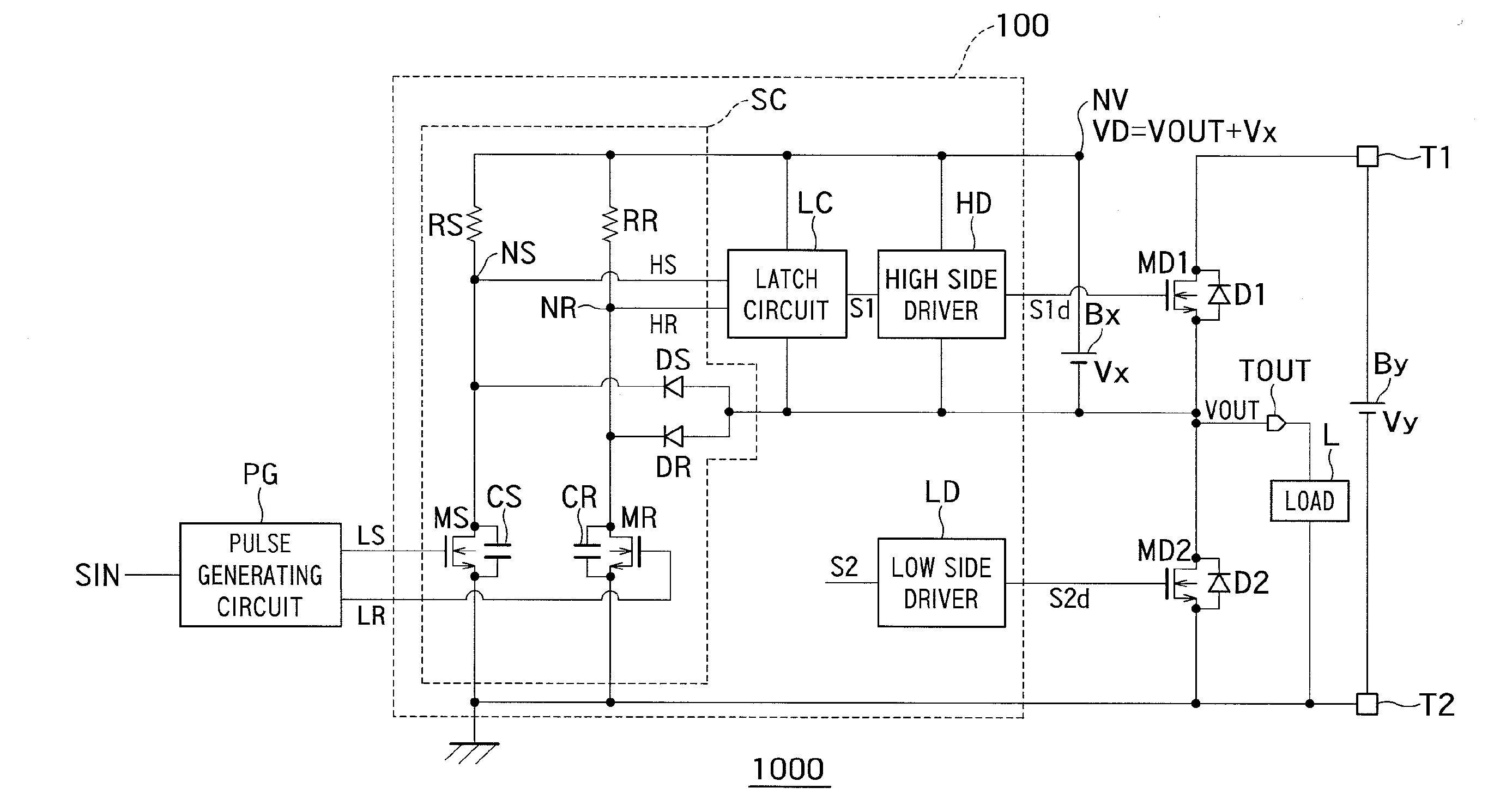
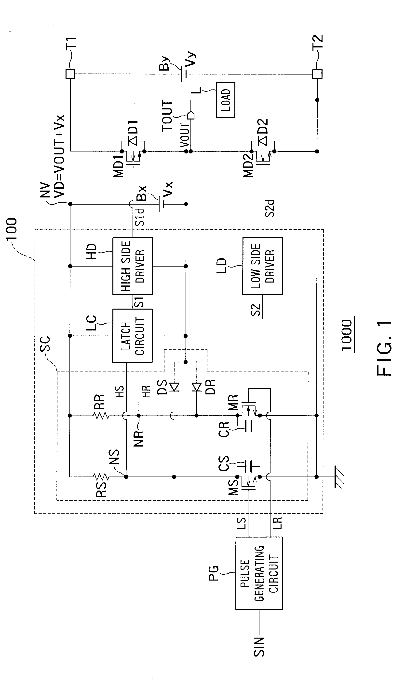
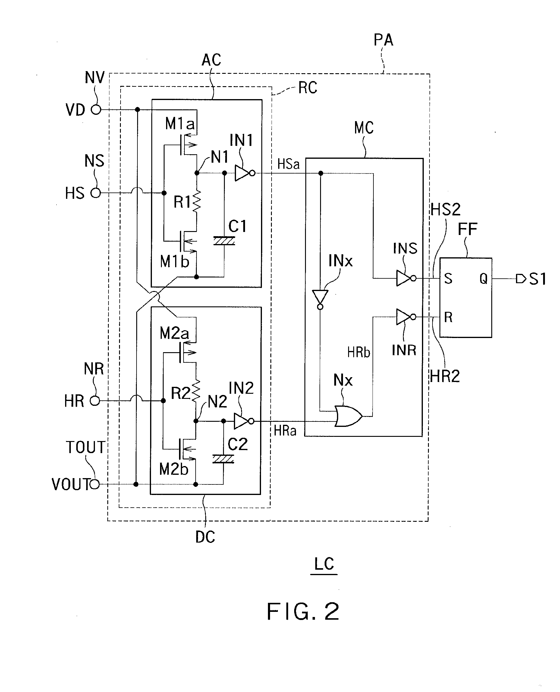
[0015]FIG. 1 is a circuit diagram showing an example of a configuration of a power semiconductor device 1000 according to a first embodiment. FIG. 2 is a circuit diagram showing an example of a configuration of a latch circuit “LC” of the power semiconductor device 1000 shown in FIG. 1.

[0016]As shown in FIG. 1, the power semiconductor device 1000 includes a driving direct-current power supply “Bx”, an output direct-current power supply “By”, an output terminal “TOUT”, a first output MOS transistor “MD1”, a second output MOS transistor “MD2”, a first output diode “D1”, a second output diode “D2”, a gate driver circuit 100, and a pulse generating circuit “PG”.

[0017]The driving direct-current power supply “Bx” outputs a power supply voltage “Vx”. The driving direct-current power supply “Bx” is connected to a power supply node (power supply terminal) “NV” at a positive electrode thereof and to the output terminal “TOUT” at a negative electrode thereof. The driving direct-current power s...


PUM


Abstract

A power semiconductor device includes a first output transistor connected to a first node at a first end of a current path thereof. The power semiconductor device further includes a second output transistor connected to a second end of the current path of the first output transistor at a first end of a current path thereof and to a second node at a second end of the current path. The power semiconductor device further includes a gate driver circuit that controls the first and second output transistors.

Description

CROSS-REFERENCE TO RELATED APPLICATION[0001]This application is based upon and claims the benefit of priority from the prior Japanese Patent Application No. 2014-185316, filed on Sep. 11, 2014, the entire contents of which are incorporated herein by reference.BACKGROUND[0002]1. Field[0003]Embodiments described herein relate generally to a power semiconductor device and a gate driver circuit.[0004]2. Background Art[0005]A conventional half-bridge gate driver circuit includes a high side driver that drives a high side switching element, a low side driver that drives a low side switching element, and a level shifting circuit that shifts the level of a low side control signal and transmits the resulting signal to the high side driver to drive the high side switching element, for example.[0006]The high side driver described above demodulates the control signal obtained by shifting the level of the input signal by means of an RS flip-flop circuit.[0007]With the RS flip-flop circuit, input...

Claims


Application Information

Patent Timeline
IPC IPC(8): H03K3/356H03K3/017
CPCH03K3/017H03K3/356113H03K17/063H03K17/162H03K2217/0063
Inventor MIWA, RYOTA
Owner KK TOSHIBA
Why Eureka
Try Eureka