Transparent display panel and method of manufacturing the same

a technology of transparent display panel and transparent plate, which is applied in the association of printed circuit non-printed electric components, instruments, dielectric characteristics, etc., can solve the problems of limiting and the aperture ratio of the transmissive portion cannot be increased, so as to increase the aperture ratio, increase the current consumption, and increase the effect of electrical resistivity

Active Publication Date: 2016-03-31
LG DISPLAY CO LTD
View PDF1 Cites 6 Cited by
  • Summary
  • Abstract
  • Description
  • Claims
  • Application Information

AI Technical Summary

Benefits of technology

[0011]Accordingly, an object of the present invention is to provide a transparent display panel including an aperture ratio that can be increased by using transparent electrodes in the transparent portion, and a method for manufacturing the same. Such transparent electrodes that can be applied in the transparent portion are made of a transparent conductive material. Because a transparent conductive material has a relatively high electrical resistivity and thus increases its current consumption, a transparent display panel with improved transmissivity and low current consumption can include transparent electrodes that still have low electrical resistivity as electrodes for a transparent portion.
[0012]Another object of the present invention is to provide a transparent display panel that includes transparent electrodes with lower electric resistivity so that current consumption can be reduced, and a method of manufacturing the same. Objects of the present invention are not limited to those described above and other objects will be clearly understood by those skilled in the art from the following descriptions.
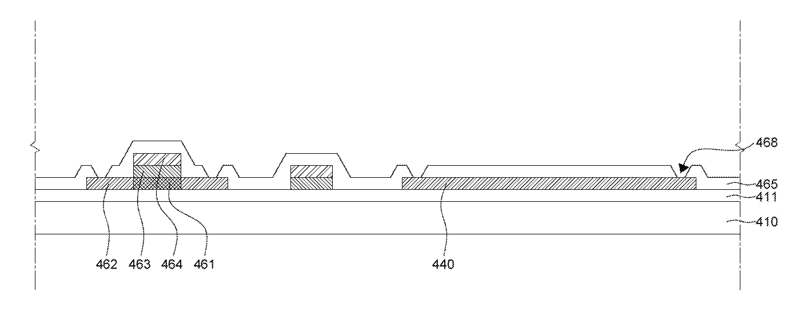
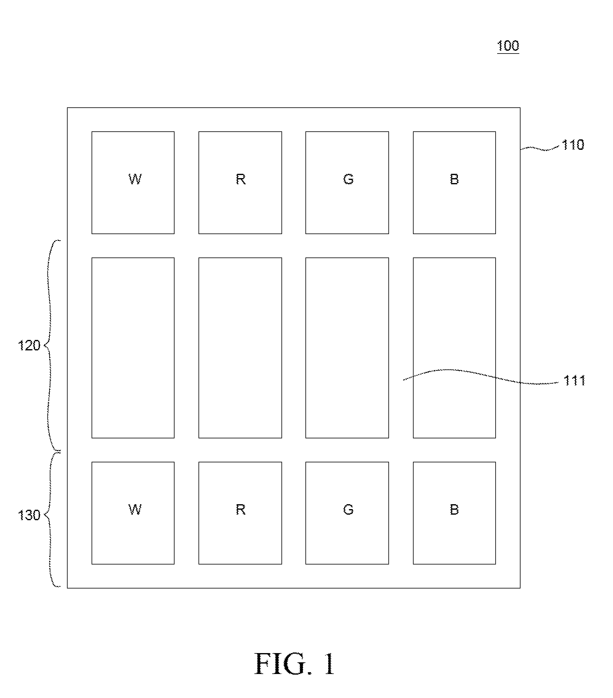
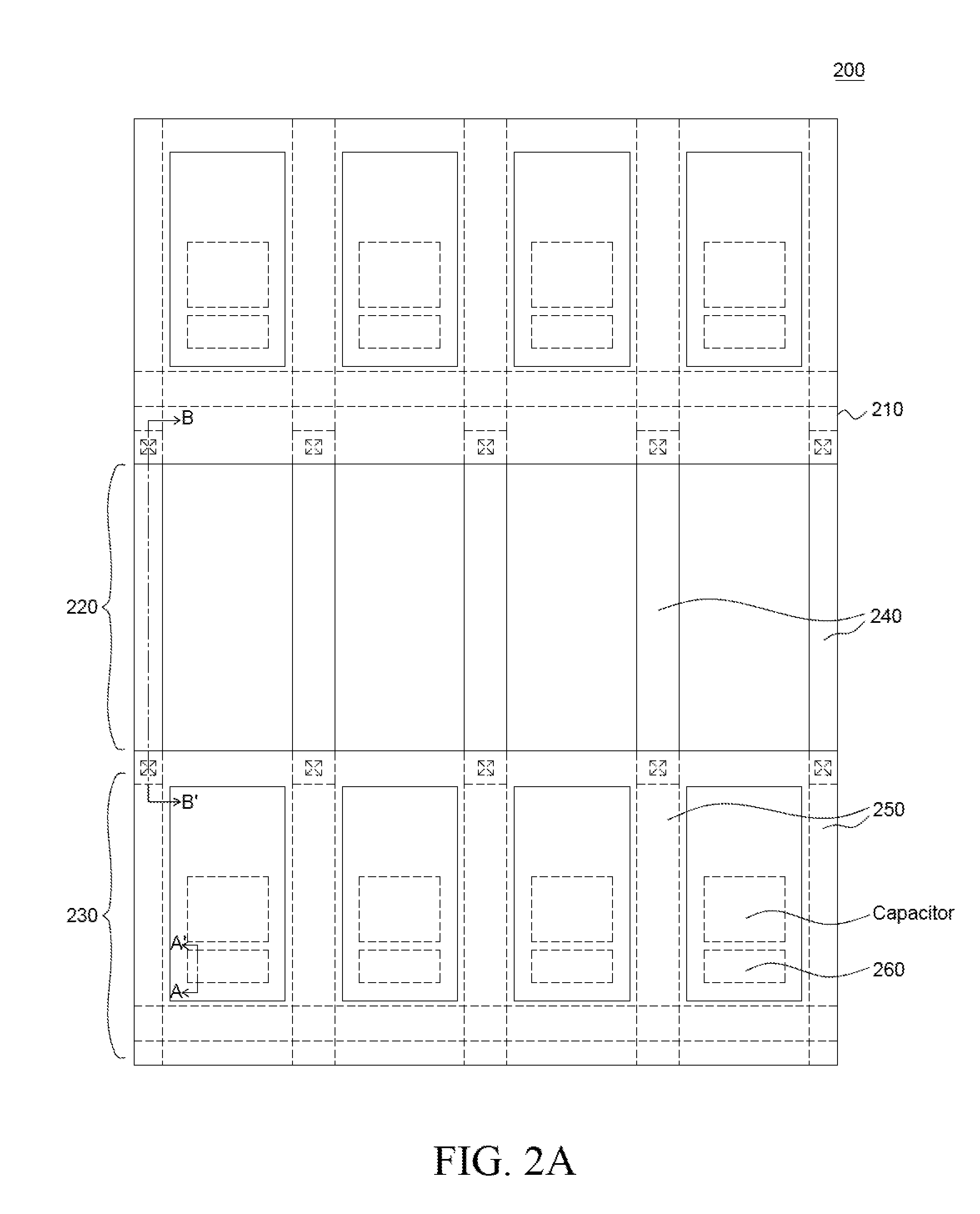
[0013]According to an aspect of the present invention, there is provided a transparent display panel with improved transmissivity by employing a transparent wiring electrode. A substrate has a transmissive area and a display pixel area defined thereon. In the display pixel area, driving elements to control the driving of display pixels, and wiring electrodes are disposed. In the transmissive area, transparent wiring electrodes conn

Problems solved by technology

The aperture ratio of the transmissive portion of the transparent display panel cannot be increased due t

Method used


Image

  • Transparent display panel and method of manufacturing the same
  • Transparent display panel and method of manufacturing the same
  • Transparent display panel and method of manufacturing the same

Examples


Embodiment Construction

[0022]Advantages and features of the present invention and methods to achieve them will become apparent from the descriptions of embodiments herein below with reference to the accompanying drawings. However, the present invention is not limited to embodiments disclosed herein but may be implemented in various different forms. The embodiments are provided for making the invention of the present invention thorough and for fully conveying the scope of the present invention to those skilled in the art. It is to be noted that the scope of the present invention is defined only by the claims.

[0023]Advantages and features of the present invention and methods to achieve them will become apparent from the descriptions of embodiments herein below with reference to the accompanying drawings. However, the present invention is not limited to embodiments disclosed herein but may be implemented in various different ways. The embodiments are provided for making the disclosure of the present inventio...


PUM


Abstract

A transparent display panel, and a method of manufacturing the transparent display panel are discussed. The transparent display panel according to one embodiment includes a substrate; a driving element formed in a display pixel area on the substrate; a wiring electrode formed in the display pixel area and connected to the driving element; and a transparent wiring electrode formed in a transmissive area on the substrate, the transparent wiring electrode being extended to connect to the wiring electrode in the display pixel area.

Description

CROSS-REFERENCE TO RELATED APPLICATIONS[0001]This application claims the priority of Korean Patent Application No. 10-2014-0130119 filed on Sep. 29, 2014, in the Korean Intellectual Property Office, the entire contents of which are incorporated herein by reference.BACKGROUND[0002]1. Field of the Invention[0003]The present invention relates to a transparent display panel capable of maximizing the aperture ratio of a transmissive portion, and a method of manufacturing the same.[0004]2. Description of the Related Art[0005]Flat display panels can have large or small screens and thus can be used in a wide range of applications. Currently, flat display panels are manufactured in a variety of types of displays and can be sorted into, for example, plasma display panels (PDPs), liquid crystal display panels (LCDs), and organic light-emitting diode display panels (OLEDs).[0006]A transparent display panel displays information thereon to viewers and also transmits light from a background so tha...

Claims


Application Information

Patent Timeline
IPC IPC(8): H05K1/09H05K1/02H05K1/18H05K3/32
CPCH05K1/0296H05K1/0274H05K1/09H05K2201/0326H05K3/32H05K2201/0108H05K1/18H05K3/388H05K2201/0175H05K2203/095H05K2203/1136G02F1/136286G02F2203/01H05K3/105G02F1/136295H10K59/121H10K59/1213H10K59/1315H01J17/49
Inventor HEO, JOONYOUNG
Owner LG DISPLAY CO LTD
Why Eureka
Try Eureka