Fin structure formation by selective etching

a selective etching and structure technology, applied in the direction of basic electric elements, electrical equipment, semiconductor devices, etc., can solve the problems of increased complexity, complicated forming of sub-10 nm node finfet structures, and difficult fabrication of high aspect ratio finfets

Active Publication Date: 2016-04-07
APPLIED MATERIALS INC
View PDF6 Cites 17 Cited by
  • Summary
  • Abstract
  • Description
  • Claims
  • Application Information

AI Technical Summary

Problems solved by technology

Fabrication of high aspect ratio FinFETs is difficult as a result of the reduced critical dimensions required for sub-10 nm nodes.
Forming sub-10 nm node FinFET structures is further complicated by limitations and increased complexities of various patterning and lithography processes.
For example, multiple patterning processes, such as self-aligned double patterning (SADP) and self-aligned quadruple patterning (SAQP) processes, may not adequately provide reliable patterning given the small pitch size requirements associated with formation of sub-10 nm node FinFET structures.
The increase in LWR may lead to variations in threshold voltages, such as “hot spots” or areas of lower resistance, of the subsequently formed fin features and ultimately result in poor device performance.
Moreover, current lithography and patterning processes are time consuming, which reduces throughput for device processing.

Method used


Image

  • Fin structure formation by selective etching
  • Fin structure formation by selective etching
  • Fin structure formation by selective etching

Examples


Embodiment Construction

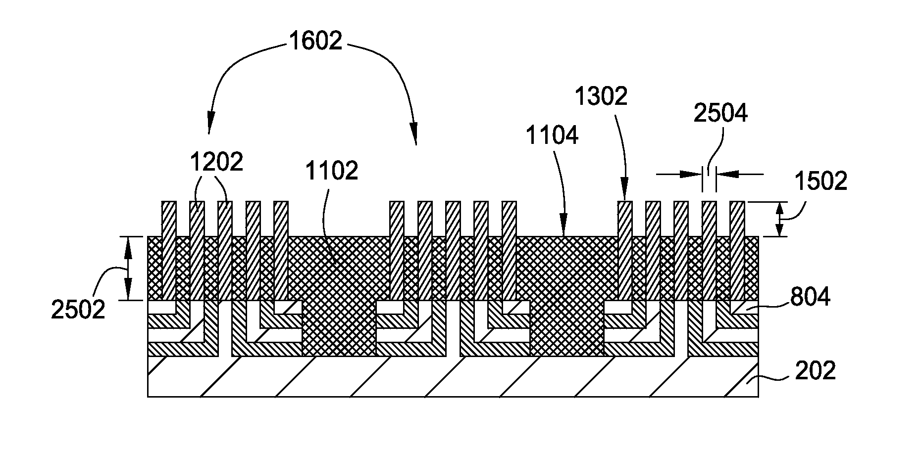
[0039]The present disclosure generally relates to methods and apparatus for forming FinFET structures. Selective etching and deposition processes described herein may provide for FinFET manufacturing while reducing or eliminating the utilization of multiple patterning processes. Embodiments described herein also provide for fin structure manufacturing methods for transitioning from silicon to III-V materials while maintaining acceptable crystal lattice orientations of the various materials utilized. Further embodiments provide etching apparatus which may be utilized to perform the methods described herein.

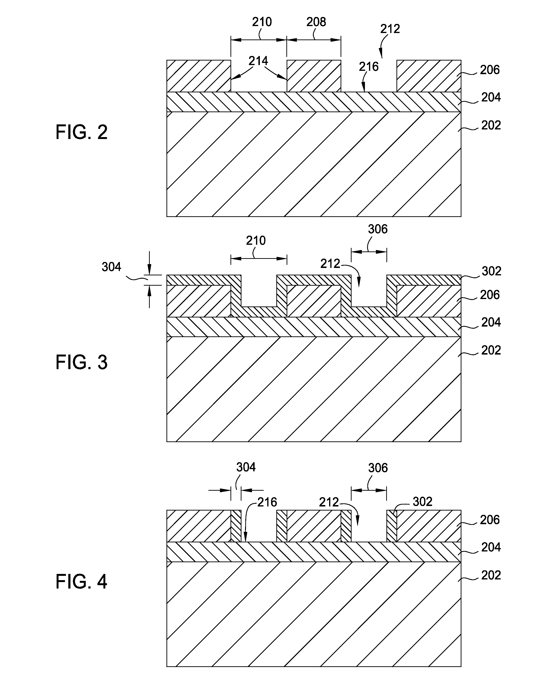
[0040]Patterning processes utilized to pattern and subsequently etch the substrate generally provide a template for superlattice structure formation. A superlattice structure as defined herein may be a two or more layers comprising different materials deposited on and adjacent one another. A thickness of one of the layer is generally several nanometers and the layers may be deposit...


PUM

PropertyMeasurementUnit
pressureaaaaaaaaaa
line width roughnessaaaaaaaaaa
thicknessaaaaaaaaaa

Abstract

Methods and apparatus for forming FinFET structures are provided. Selective etching and deposition processes described herein may provide for FinFET manufacturing without the utilization of multiple patterning processes. Embodiments described herein also provide for fin material manufacturing methods for transitioning from silicon to III-V materials while maintaining acceptable crystal lattice orientations of the various materials utilized. Further embodiments provide etching apparatus which may be utilized to perform the methods described herein.

Description

CROSS-REFERENCE TO RELATED APPLICATIONS[0001]This application claims benefit of U.S. Provisional Patent Application No. 62 / 059,932, filed Oct. 5, 2014, the entirety of which is herein incorporated by reference.BACKGROUND[0002]1. Field[0003]Embodiments of the present disclosure generally relate to methods and apparatus for forming fin field-effect transistor (FinFETs) structures. More specifically, embodiments described herein relate to fin structure formation by selective etching and deposition processes.[0004]2. Description of the Related Art[0005]In response to an increased need for smaller electronic devices with denser circuits, devices with three dimensional (3D) structures have been developed. An example of such devices may include FinFETs having conductive fin-like structures that are raised vertically above a horizontally extending substrate. Conventional FinFETs may be formed on a substrate, such as a semiconducting substrate or silicon-on-insulator substrates. The substrat...

Claims


Application Information

Patent Timeline
Patent Type & Authority Applications(United States)
IPC IPC(8): H01L21/8234H01L21/02H01L21/8258H01L21/306
CPCH01L21/823431H01L21/30604H01L21/02538H01L21/8258H01L21/0245H01L21/02507H01L21/02381H01L21/02532H01L21/02639H01L21/02164H01L21/02274H01L21/3065H01L21/3086H01L21/31116H01L29/66795
Inventor ZHANG, YINGCHUNG, HUA
Owner APPLIED MATERIALS INC
Why Eureka
Try Eureka