

Semiconductor memory device
- Summary
- Abstract
- Description
- Claims
- Application Information
AI Technical Summary
Benefits of technology
Problems solved by technology
Method used
Image

Examples
first embodiment
[0088]Next, a description will be given of a bit line non-precharge method, in which the bit line and the inverted bit line are not precharged during a read / write operation.
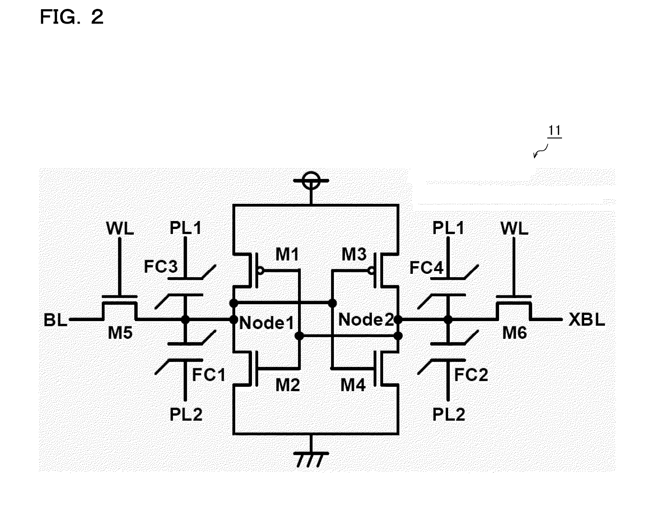
[0089]FIG. 4 is a diagram illustrating the necessity for bit line precharging in an SRAM memory cell having a 6T structure. As shown there, a plurality of SRAM memory cells 11-1 and 11-2 belonging to the same row are all connected to a single word line WL. On the other hand, a plurality of SRAM memory cells 11-1 and 11-2 belonging to different columns are respectively connected to corresponding bit lines BL1 and BL2 and to corresponding inverted bit lines XBL1 and XBL2.
[0090]In a read / write operation in the SRAM memory cell 11-1, the word line WL is raised to high level. As a result, the SRAM memory cell 11-1 that is a target of the read / write operation becomes connected to the corresponding bit line BL1 and inverted bit line XBL1. Here, the word line WL is connected also to the SRAM memory cell 11-2 that is not ...
second embodiment
[0111]Next, a description will be given of a plate line charge share method in which electric charge is shared between plate lines PL1 and PL2 that are sequentially driven in a store / recall operation.
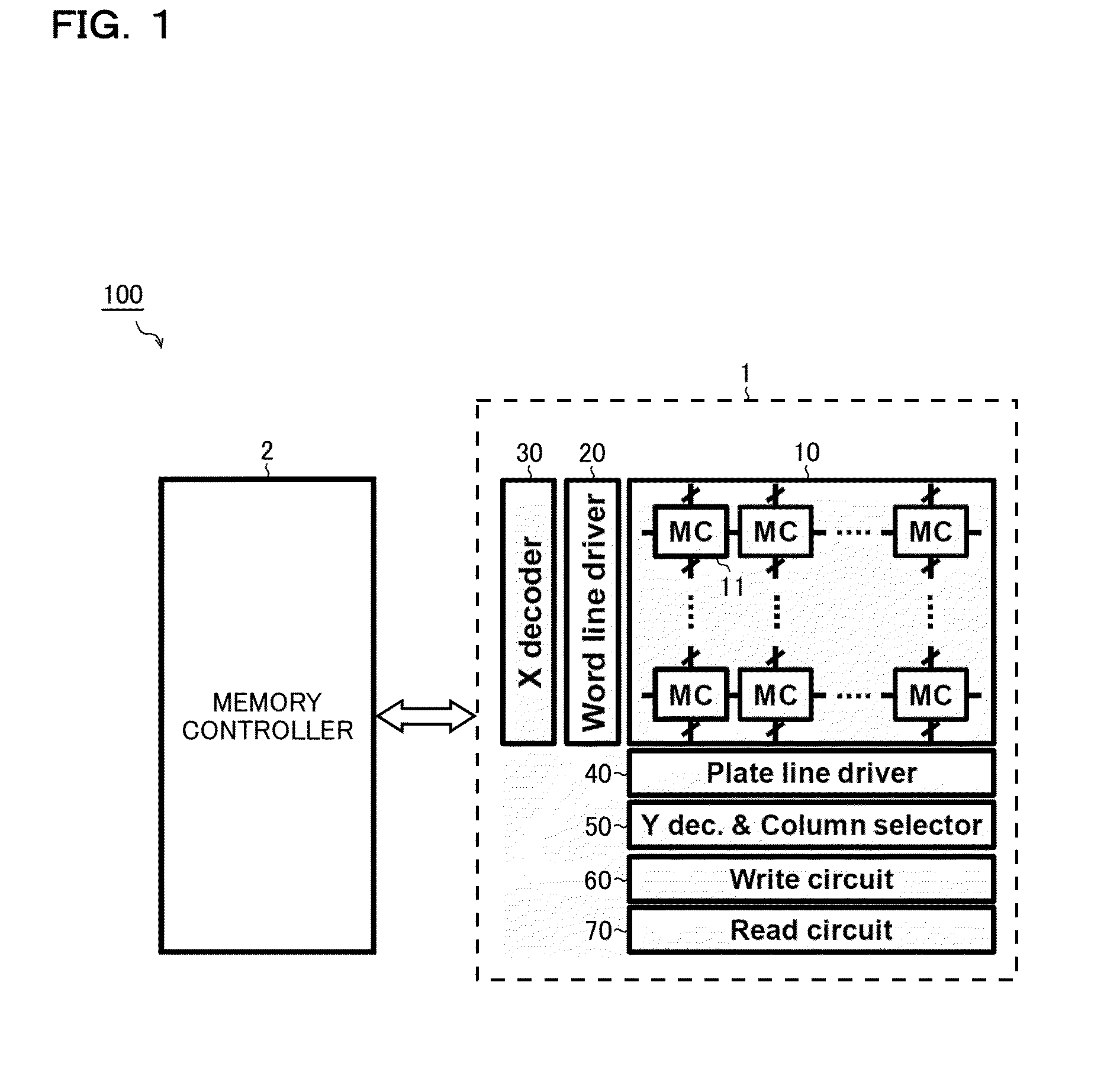
[0112]FIG. 9 is a diagram showing one example of configuration for achieving the plate line charge share method. The semiconductor memory device 100 of this configuration example includes, as described previously, a plurality of memory cells 11 arrayed in a matrix, plate lines PL1(a, b, . . . ) and PL2(a, b, . . . ) connected to the plurality of memory cells 11 respectively, a plate line driver 40 for driving the plate lines PL1(a, b, . . . ) and PL2(a, b, . . . ) individually, and a memory controller 2 for controlling access to the plurality of memory cells 11.
[0113]The semiconductor memory device 100 of this configuration example further includes a plurality of transmission gates SW1(ab, bc, . . . ) and SW2(ab, bc, . . . ) commented between adjacent plate lines. Specifically, a transm...
third embodiment
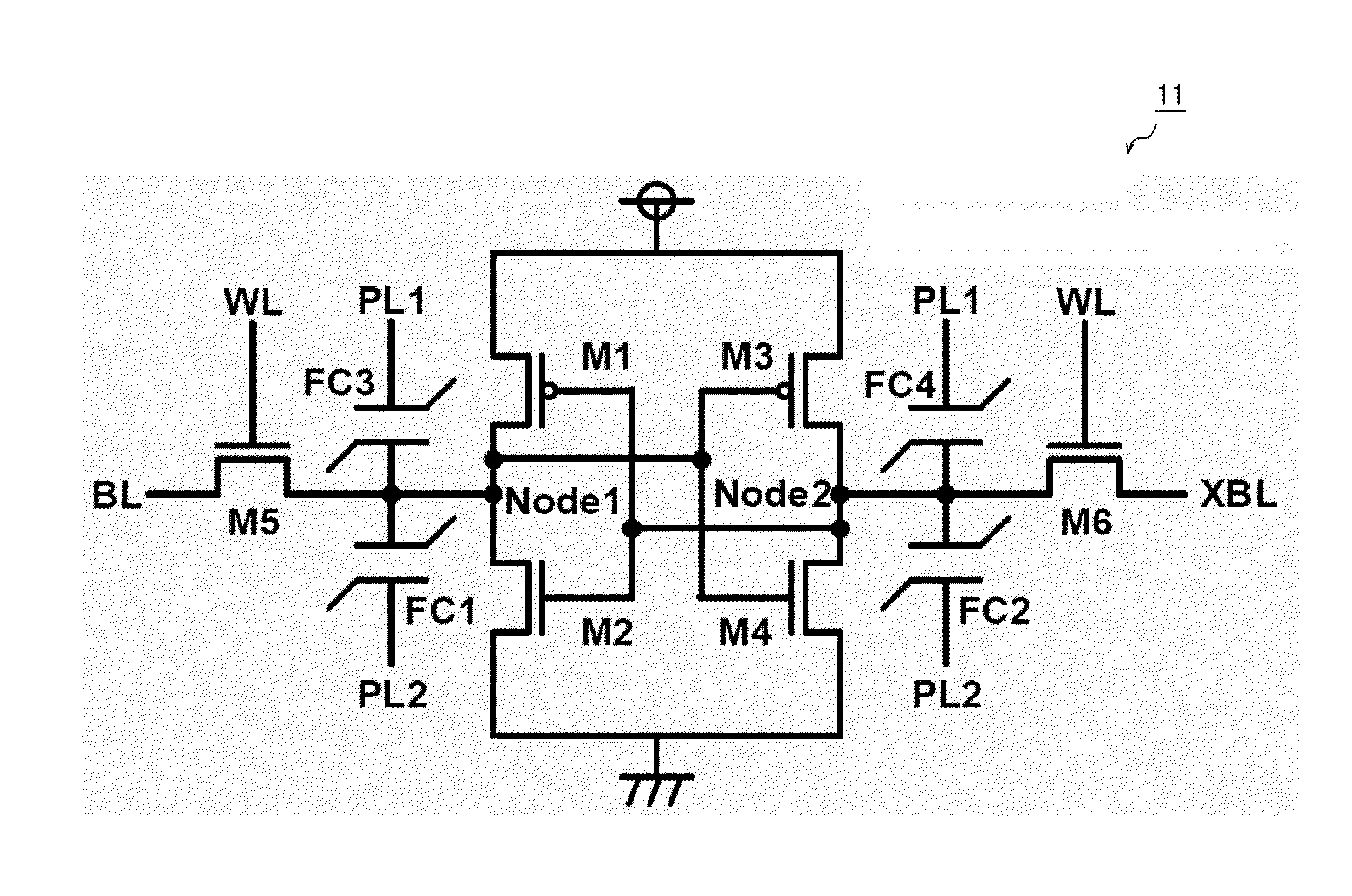
[0127]As shown in FIG. 2 previously referred to, in a ferroelectric shadow memory having a 6T-4C structure, internal nodes Node1 and Node2 are connected to ferroelectric capacitors FC1 to FC4 with a high capacitance. Thus, with a ferroelectric shadow memory, data writing during an active period requires longer time than with an SRAM having a 6T structure. As a solution to this problem, a description will be given below of a word line boost method in which the potential on a word line WL is raised in a write operation.
[0128]FIG. 12 is a circuit diagram showing one example of the configuration of the word line driver 20. The word line driver 20 of this configuration example includes P-channel type field-effect transistors 21 and 22, an N-channel type field-effect transistor 23, an inverter 24, and a capacitor element 25.
[0129]The source of the transistor 21 is connected to a supply voltage node. The drain of the transistor 21 is connected to the source of the transistor 22. The drains...
PUM
 Abstract
Description
Claims
Application Information