Common mode filter and esd-protection-circuit-equipped common mode filter

a common-mode filter and protection circuit technology, applied in the direction of impedence networks, emergency protective arrangements for limiting excess voltage/current, inductance, etc., can solve the problem of low self-resonant frequency, large transmission loss of signals, and difficulty in using a common-mode choke coil in differential transmission lines that are used in high frequency, etc. problem, to achieve the effect of small coupling coefficient, small inductance and small coupling coefficien

Active Publication Date: 2016-05-19
MURATA MFG CO LTD
View PDF2 Cites 15 Cited by
  • Summary
  • Abstract
  • Description
  • Claims
  • Application Information

AI Technical Summary

Benefits of technology

[0021]According to various preferred embodiments of the present invention, a common mode filter and an ESD-protection-circuit-equipped common mode filter, despite having a small inductance and a small coupling coefficient, are highly effective at suppressing common mode noise, have excellent characteristics at high frequencies and have small transmission loss.

Problems solved by technology

However, when the inductances of the coils are large and the coupling coefficient between the coils is large, the self-resonant frequency is low and the transmission loss of a signal is large.
Consequently, it is difficult to use such a common-mode choke coil in a differential transmission line that is used in a high frequency band and that is required to have low transmission loss such as a differential transmission line for a high-speed interface like USB or HDMI (registered trademark), for example.

Method used


Image

  • Common mode filter and esd-protection-circuit-equipped common mode filter
  • Common mode filter and esd-protection-circuit-equipped common mode filter
  • Common mode filter and esd-protection-circuit-equipped common mode filter

Examples


first preferred embodiment

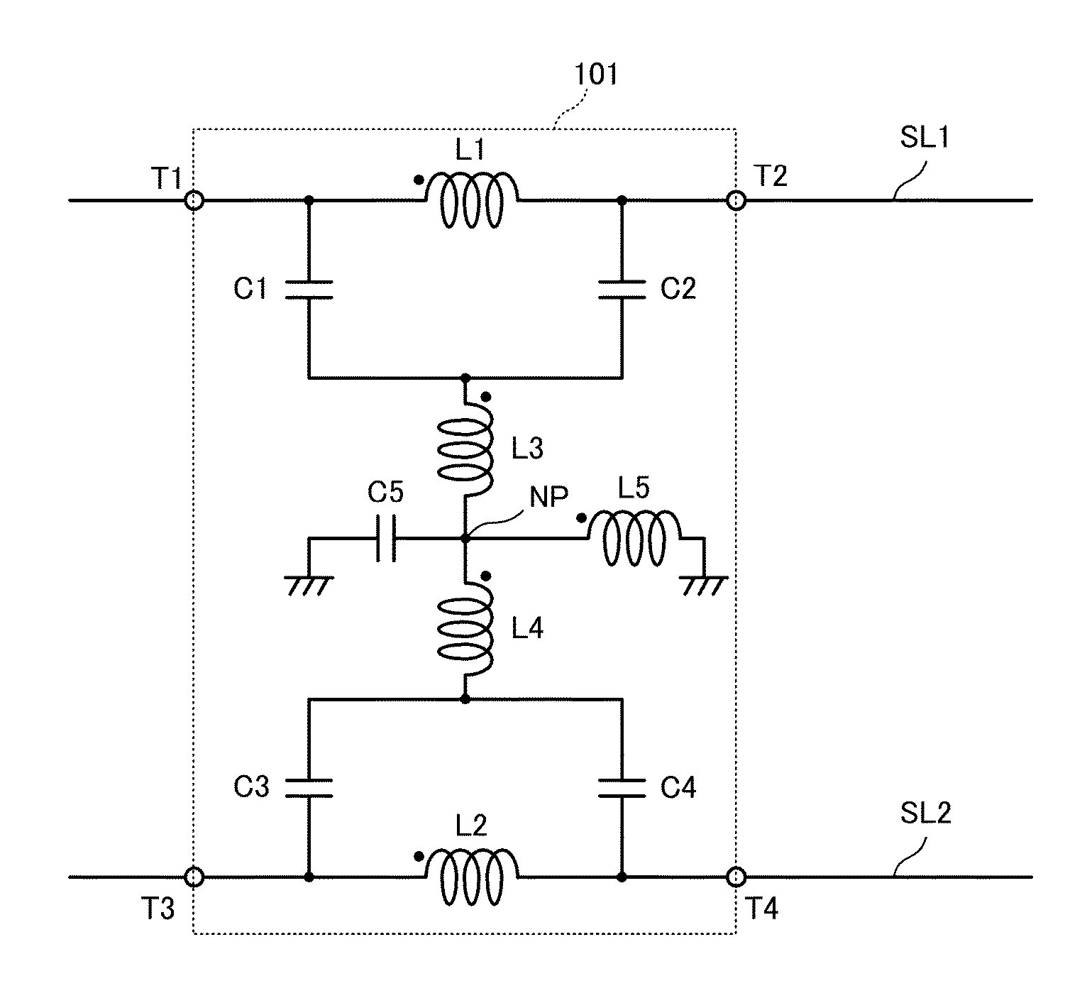
[0040]A common mode filter according to a first preferred embodiment of the present invention will be described with reference to the drawings. FIG. 1 is a circuit diagram of a common mode filter 101 of the first preferred embodiment.

[0041]The common mode filter 101 illustrated in FIG. 1 is a balanced filter that is connected to a differential transmission line including a first signal line SL1 and a second signal line SL2. A first inductance element (hereafter, “first inductor”) L1 is inserted in series with the first signal line SL1 and a second inductance element (hereafter, “second inductor”) L2 is inserted in series with the second signal line SL2. The common mode filter 101 is provided with a ground that defines and functions as a reference for the first signal line SL1 and the second signal line SL2. In addition, the common mode filter 101 includes a third inductance element (hereafter, “third inductor”) L3, which includes a first end connected to a neutral point NP with resp...

second preferred embodiment

[0079]In a second preferred embodiment of the present invention, an example is illustrated in which characteristics are determined by the coupling of the third inductor L3 and the fourth inductor L4.

[0080]A circuit diagram of a common mode filter according to the second preferred embodiment is the same as that illustrated in FIG. 1 for the first preferred embodiment. In FIG. 1, when adopting a configuration in which the third inductor L3 and the fourth inductor L4 are coupled with each other, there is a configuration in which the inductors are differentially coupled for a common mode current and cumulatively coupled for a differential mode current (hereafter, “differential coupling”), and conversely, there is a configuration in which the inductors are cumulatively coupled for a common mode current and differentially coupled for a differential mode current (hereafter, “cumulative coupling”).

[0081]FIG. 10A illustrates frequency characteristics of the common mode filter when the differ...

third preferred embodiment

[0085]In a third preferred embodiment of the present invention, an example is illustrated in which a common mode filter is provided in a re-wiring layer of a semiconductor substrate.

[0086]FIG. 12 is a perspective view of an ESD-protection-circuit-equipped common mode filter according to the third preferred embodiment. A structure defined by a plurality of layers is illustrated and therefore the thickness in the stacking direction is drawn in an exaggerated manner. FIG. 13 is a plan view of each layer of the re-wiring layer. FIG. 14 is a circuit diagram of the ESD-protection-circuit-equipped common mode filter of this preferred embodiment.

[0087]FIG. 12 specifically illustrates a re-wiring layer RL provided on a surface of a semiconductor substrate SUB. In FIG. 12, a surface SS is the surface of the semiconductor substrate and is a surface below the re-wiring layer. Bidirectional Zener diodes ZD1 and ZD2 are defined by p-diffusion layers and re-diffusion layers in the semiconductor su...


PUM


Abstract

On a first-signal-line side, a first resonant circuit is defined by a first inductance element, a first capacitance element, a second capacitance element, a third inductance element and a fifth inductance element, a third resonant circuit is defined by the first inductance element, the first capacitance element and the second capacitance element, and a fifth resonant circuit is defined by the first inductance element, the third inductance element, the first capacitance element, the second capacitance element and the fifth capacitance element. Similarly, on a second-signal-line side, a second resonant circuit, a fourth resonant circuit and a sixth resonant circuit are provided.

Description

BACKGROUND OF THE INVENTION[0001]1. Field of the Invention[0002]The present invention relates to a common mode filter that suppresses common mode noise that propagates through a differential transmission line, and to an ESD-protection-circuit-equipped common mode filter.[0003]2. Description of the Related Art[0004]Conventionally, a common-mode choke coil is used to suppress common mode noise attempting to propagate through a differential transmission line. A common-mode choke coil includes two coils, the two coils being configured such that magnetic fields generated around the coils by differential mode signals (normal mode signals) cancel each other out and the magnetic fields strengthen each other for common mode signals (common mode noise), as described in Japanese Unexamined Patent Application Publication No. 2003-133135, for example.[0005]Generally, it is necessary that the coils each have a large inductance and that there be a large coupling coefficient between the coils in su...

Claims


Application Information

Patent Timeline
Patent Type & Authority Applications(United States)
IPC IPC(8): H03H7/01H02H9/04
CPCH02H9/045H03H7/0115H03H7/09H01F2017/0026H03H7/427H02H9/046
Inventor UEKI, NORIYUKIAKIYAMA, HISASHI
Owner MURATA MFG CO LTD
Why Eureka
Try Eureka