Reverse conducting semiconductor device

Active Publication Date: 2016-05-26
MITSUBISHI ELECTRIC CORP
View PDF0 Cites 6 Cited by
  • Summary
  • Abstract
  • Description
  • Claims
  • Application Information

AI Technical Summary

Benefits of technology

[0009]According to one aspect of the present invention, a reverse conducting semiconductor device includes a semiconductor substrate of a first conduction type having a first major surface and a second major surface, gate electrodes formed in a plurality of trenches provided in stripe form in the first major surface, with a gate oxide film interposed between the gate electrodes and the trenches, a transistor having an emitter layer formed on the first major surface side, a base layer of a second conduction type formed below the emitter layer and bordering the gate oxide film, and a collector layer of the second conduction type formed on the second major surface side, a diode having an anode layer of the second conduction type formed on the first major surface side, a high-concentration anode layer of the second conduction type formed on the first major surface side and having an impurity concentration higher than th

Problems solved by technology

If the trench gate interval is reduced, it is difficult to connect the anode layer and the emitter electrode by a contact electrode formed of aluminum for example.
Therefore, if the p+-anode layer (a high-concentration anode layer) is formed in island f

Method used


Image

  • Reverse conducting semiconductor device
  • Reverse conducting semiconductor device
  • Reverse conducting semiconductor device

Examples


first embodiment

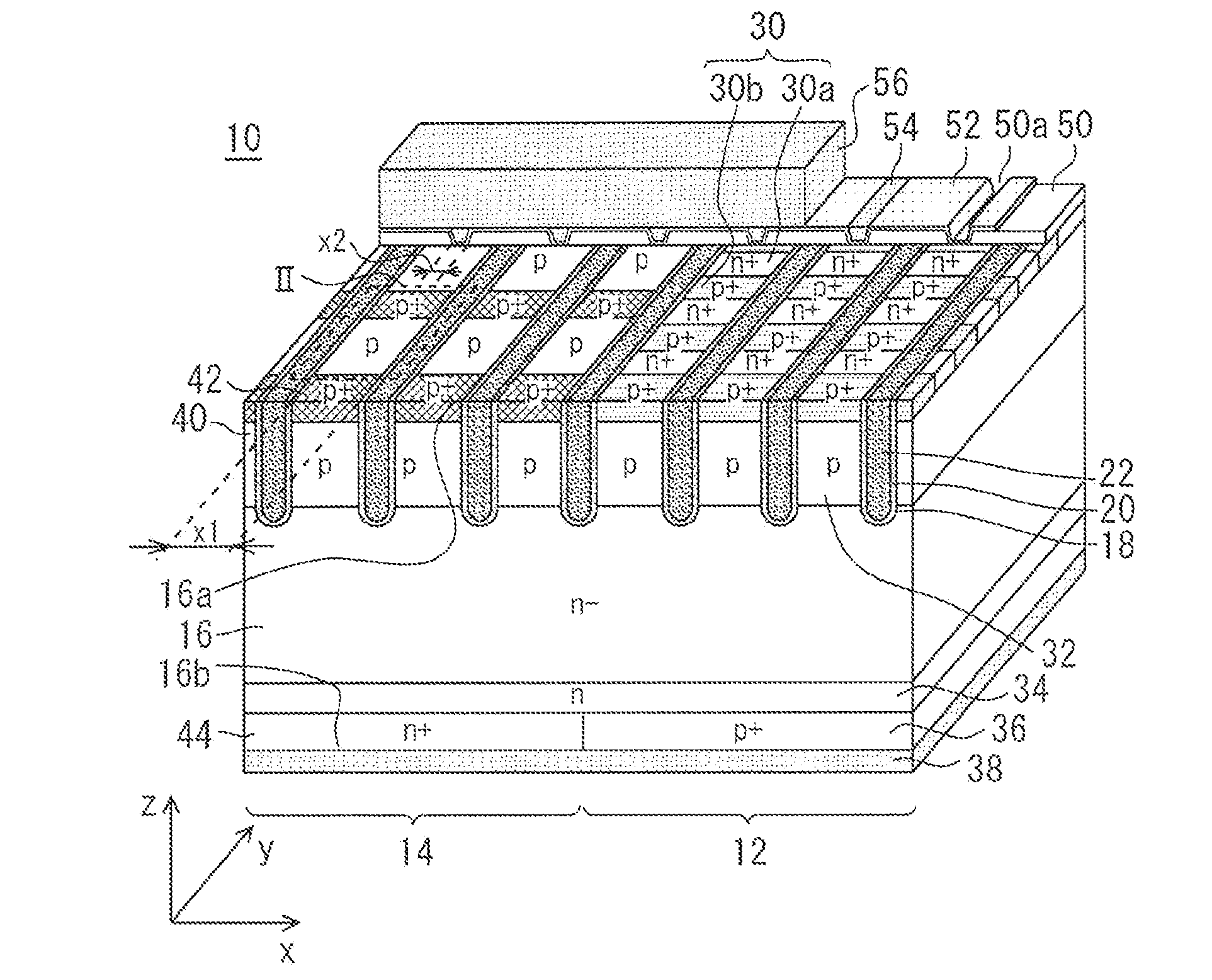
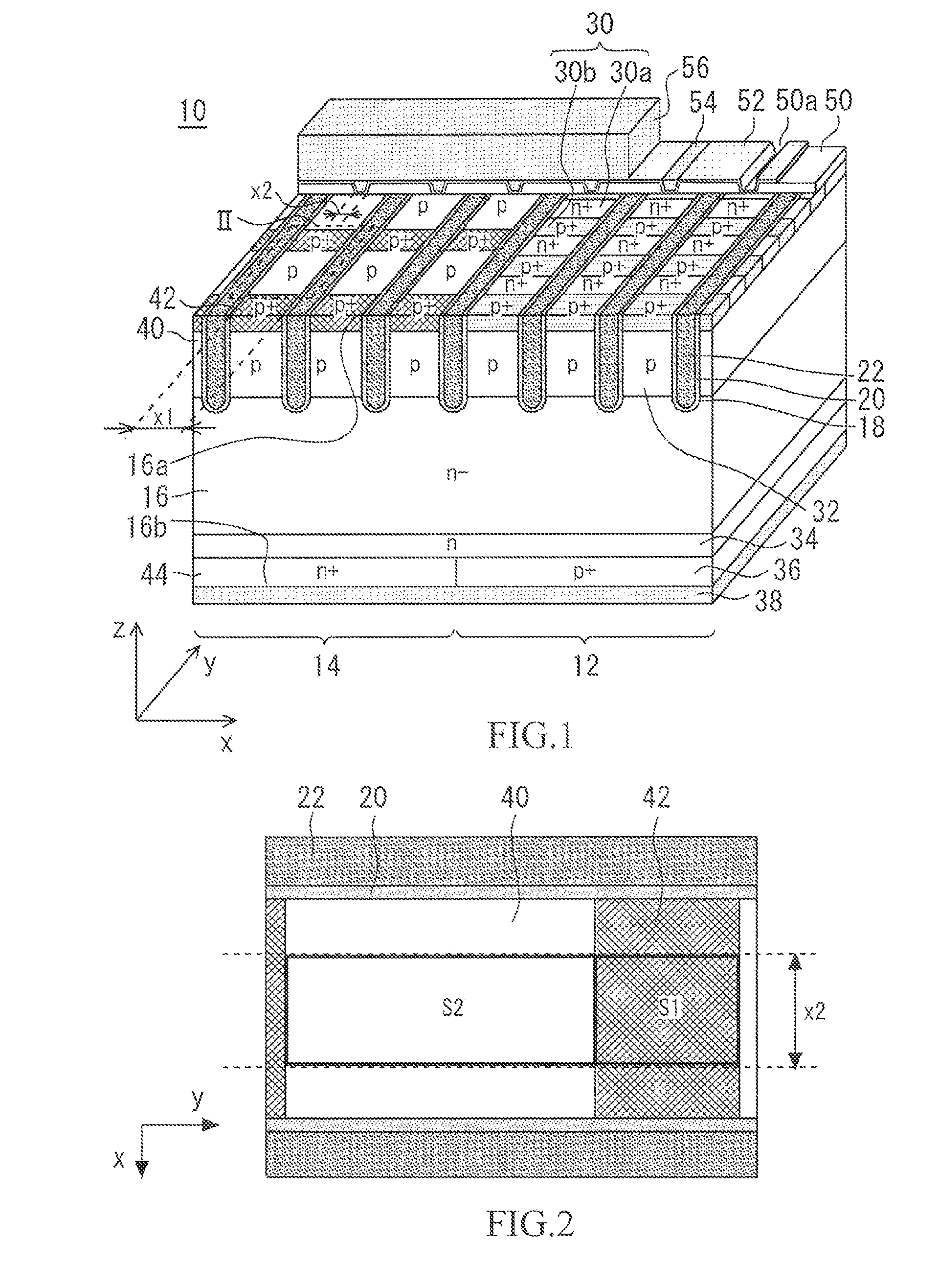
[0018]FIG. 1 is a perspective view of a reverse conducting semiconductor device 10 according to a first embodiment of the present invention. The reverse conducting semiconductor device 10 has a transistor 12 and a diode 14 formed horizontally adjacent to the transistor 12. The transistor 12 and the diode 14 are formed on a semiconductor substrate 16. The semiconductor substrate 16 is a first conduction type (n-type) of substrate having a first major surface 16a and a second major surface 16b.

[0019]A plurality of trenches 18 in stripe form are provided in the first major surface 16a. A gate oxide film 20 is formed on inner wall surfaces of the trenches 18. The trenches 18 have gate electrodes 22 formed therein, filling the trenches 18 and bordering the gate oxide film 20. The gate electrodes 22 are formed of polysilicon for example. The trenches 18, the gate oxide film 20 and the gate electrodes 22 are formed both in the transistor 12 and in the diode 14.

[0020]The transistor 12 has ...

second embodiment

[0038]FIG. 6 is a perspective view of a reverse conducting semiconductor device according to a second embodiment of the present invention. The reverse conducting semiconductor device according to the second embodiment have a number of commonalities with the first embodiment and will therefore be described with respect to points of difference from the first embodiment. Segments of a high-concentration anode layer 100 are disposed in a staggered pattern as viewed in plan. That is, the high-concentration anode layer 100 is formed in zigzag such that each segment of the high-concentration anode layer does not border any of the other segments through the gate oxide film 20 and the gate electrode 22.

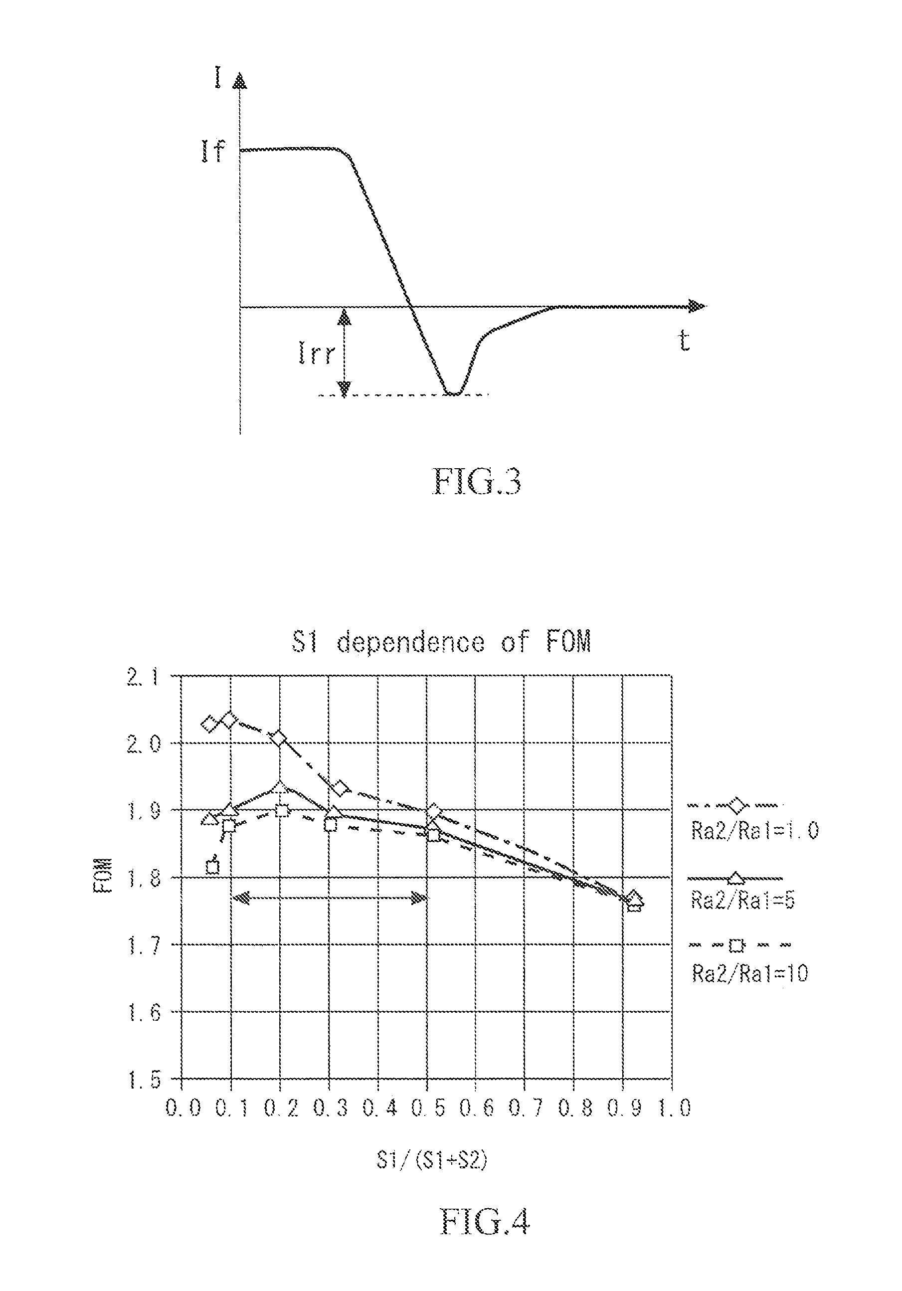
[0039]Disposing segments of a high-concentration anode layer 100 in a staggered pattern as viewed in plan enables uniformization of the current distribution in the diode 14. Prevention of a local increase in temperature of the diode 14 at a particular position can be achieved by uniformizing t...


PUM


Abstract

A reverse conducting semiconductor device includes a high-concentration anode layer and a barrier metal layer, the width of the high-concentration anode layer is set larger than the width of contact of the barrier metal layer and the high-concentration anode layer, thereby ensuring that the area of contact between the barrier metal layer and the high-concentration anode layer is constant.

Description

BACKGROUND OF THE INVENTION[0001]1. Field of the Invention[0002]The present invention relates to a reverse conducting semiconductor device for use in home electric appliances, electric motor vehicles, railroad systems, solar or wind power systems, etc.[0003]2. Background Art[0004]Japanese Patent Laid-Open No. 2013-197122 discloses a reverse conducting semiconductor device (a reverse conducting insulated gate bipolar transistor (RC-IGBT)). The reverse conducting semiconductor device has an IGBT and a diode (free wheeling diode (FWD)) formed on one semiconductor substrate. In the reverse conducting semiconductor device disclosed in Japanese Patent Laid-Open No. 2013-197122, a p-anode layer and a p+-anode layer are provided as an anode layer for the diode and an ohmic contact is established between the p+-anode layer and an emitter electrode.[0005]In a case where trench gates are formed in the entire surface of the semiconductor substrate, the trench gate interval may be reduced in ord...

Claims


Application Information

Patent Timeline
IPC IPC(8): H01L27/06H01L23/535H01L29/20H01L29/417H01L29/10H01L29/16H01L29/739H01L23/532
CPCH01L27/0635H01L29/7397H01L23/535H01L23/53266H01L29/1602H01L29/1095H01L29/1608H01L29/2003H01L29/417H01L27/0688H01L27/0727H01L29/0696H01L29/0834
Inventor SONEDA, SHINYA
Owner MITSUBISHI ELECTRIC CORP
Why Eureka
Try Eureka