
Solid-state imaging device

Inactive Publication Date: 2016-06-02
CANON KK
View PDF5 Cites 3 Cited by
  • Summary
  • Abstract
  • Description
  • Claims
  • Application Information

AI Technical Summary

Benefits of technology

The patent aims to improve the speed of a solid-state imaging device by allowing it to quickly read out a signal from a pixel's amplifier unit to a signal line.

Problems solved by technology

However, according to the technique disclosed in Japanese Patent Application Laid-Open No. 2013-243781, although a parasitic capacitance of the vertical signal line can be reduced by dividing the vertical signal lines, since two signal processing circuits are necessary, a circuit area necessary for the signal processing circuits increases and their control also becomes complicated.

Method used


Image

  • Solid-state imaging device
  • Solid-state imaging device
  • Solid-state imaging device

Examples


first embodiment

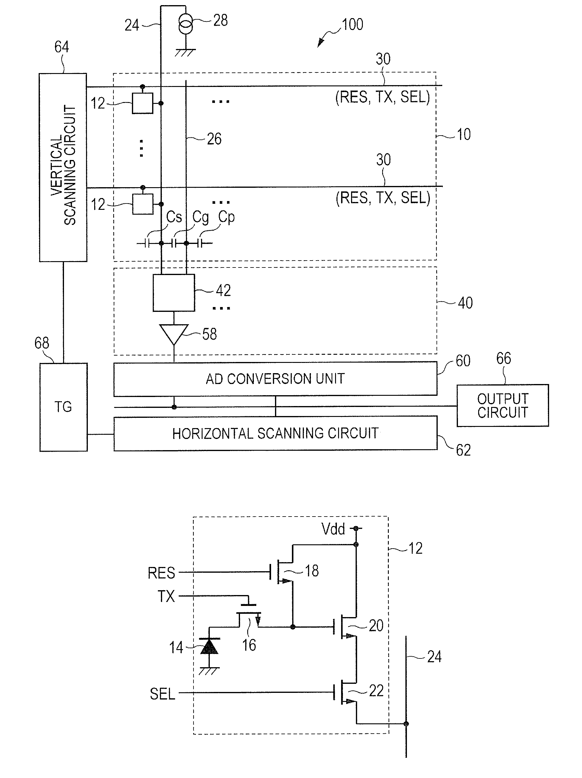
[0016]A solid-state imaging device according to a first embodiment of the present invention will be described hereinbelow with reference to FIGS. 1A to 4.

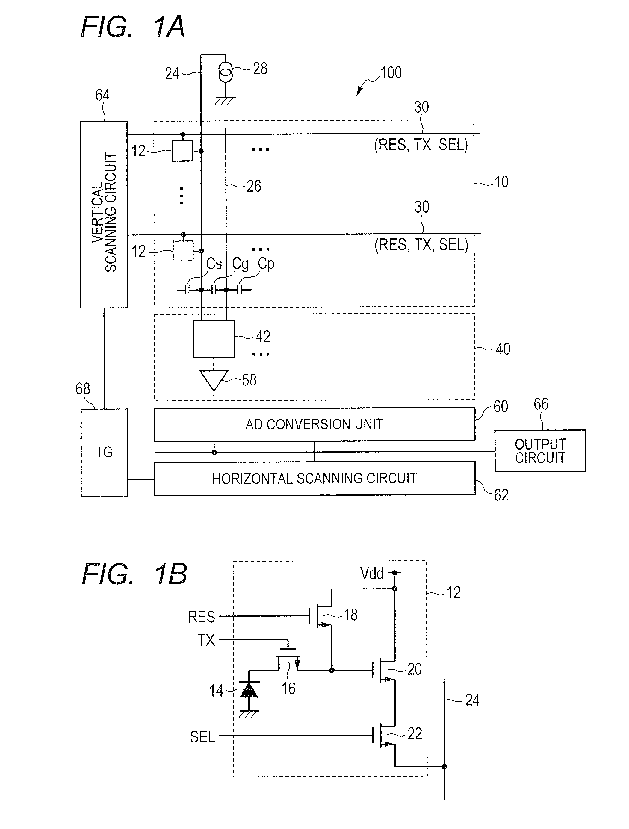
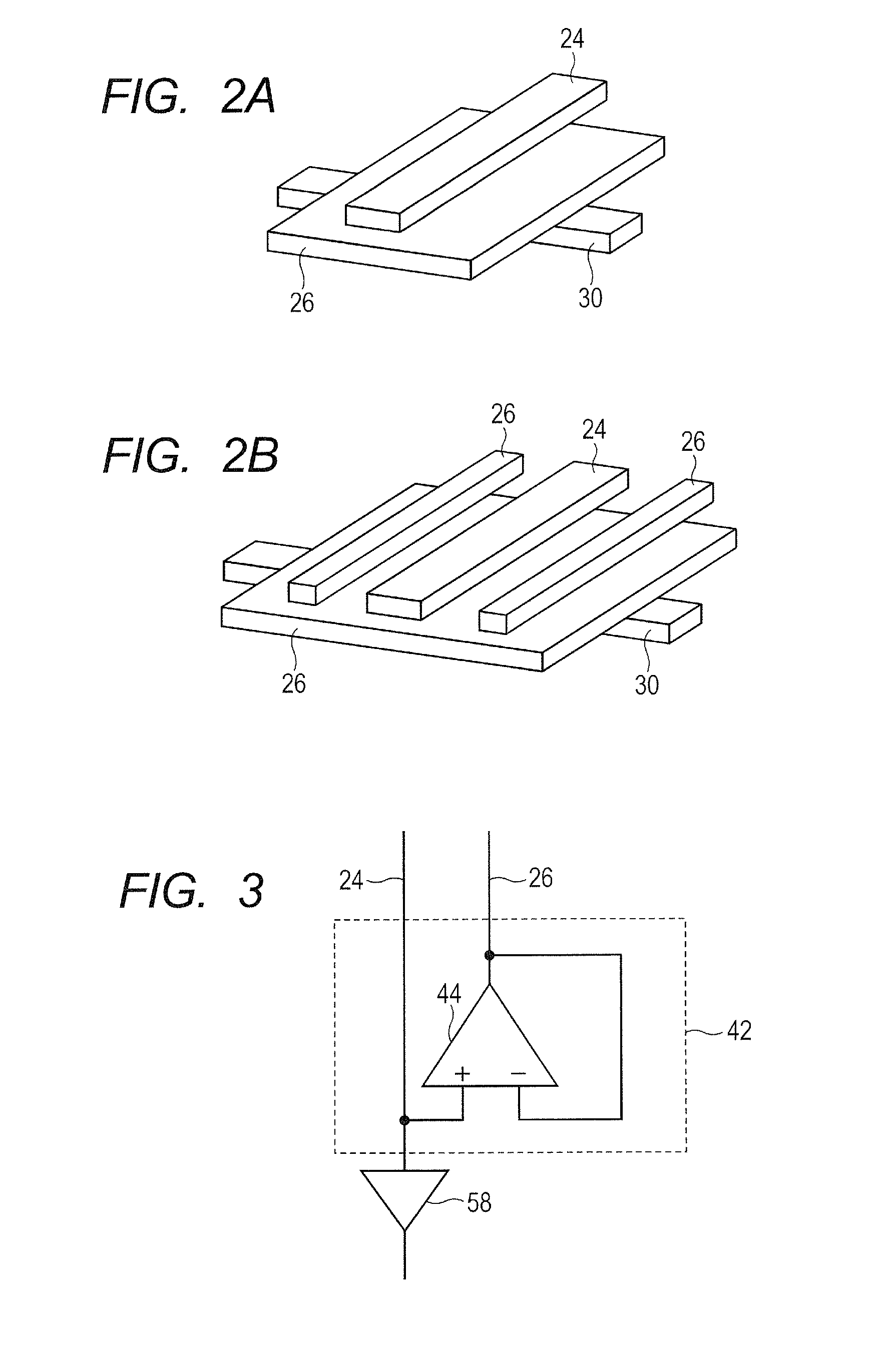
[0017]FIGS. 1A and 1B are schematic diagrams illustrating a construction of the solid-state imaging device according to the present embodiment. FIGS. 2A and 2B are perspective views each illustrating an example of a layout of guard lines in the solid-state imaging device according to the present embodiment. FIG. 3 is a diagram illustrating a circuit construction of an amplifying processing unit of the solid-state imaging device according to the present embodiment. FIG. 4 is a timing chart illustrating the operation of the solid-state imaging device according to the present embodiment.

[0018]First, a structure of the solid-state imaging device according to the present embodiment will be described with reference to FIGS. 1A to 3. FIG. 1A is a diagram illustrating a general construction of the solid-state imaging device according to th...

second embodiment

[0051]A solid-state imaging device according to a second embodiment of the present invention will be described hereinbelow with reference to FIGS. 5A and 5B. Component elements similar to those in the solid-state imaging device according to the first embodiment illustrated in FIGS. 1A to 4 are designated by the same reference numerals and their description is omitted or simplified.

[0052]FIGS. 5A and 5B are diagrams illustrating a circuit construction of the buffer amplifier unit 42 of the solid-state imaging device according to the present embodiment. FIG. 5A illustrates a connection relation between the general construction of the buffer amplifier unit 42 and signal lines. FIG. 5B illustrates an example of a construction of a high pass filter 56 connected to the buffer amplifier unit 42.

[0053]As illustrated in FIG. 5A, the buffer amplifier unit 42 of the solid-state imaging device according to the present embodiment has a buffer amplifier 46, an inverting amplifier 48, and an inver...

third embodiment

[0062]An imaging system according to a third embodiment of the present invention will be described with reference to FIG. 6.

[0063]FIG. 6 is a schematic diagram illustrating an example of a construction of the imaging system according to the present embodiment. Component elements similar to those in the solid-state imaging devices according to the first and second embodiments illustrated in FIGS. 1A to 5B are designated by the same reference numerals and their description is omitted or simplified.

[0064]An imaging system 200 according to the present embodiment can be applied to, for example, a digital still camera, a digital camcorder, a camera head, a copying apparatus, a facsimile apparatus, a cellular phone, an onboard camera, an observation satellite, and the like although it is not particularly limited.

[0065]The imaging system 200 has the solid-state imaging device 100, a lens 202, an aperture 203, a barrier 201, a signal processing unit 207, a timing generating unit 208, a gener...


PUM


Abstract

A solid-state imaging device includes a plurality of pixels each including a photoelectric converting element and an amplifier unit for outputting a signal based on charges generated by the photoelectric converting element, a signal line connected to the plurality of pixels, a second line arranged at a position adjacent to the signal line, and a buffer unit connected to the signal line. The buffer unit buffers the signal at to the signal line, and outputs a signal having a same phase as that of the signal to the second line.

Description

BACKGROUND OF THE INVENTION[0001]1. Field of the Invention[0002]The present invention relates to a solid-state imaging device.[0003]2. Description of the Related Art[0004]In association with an increase in number of pixels of an imaging area of a solid-state imaging device and an enlargement of a photosensitive area, a technique for reading out a pixel signal at a higher speed is demanded. Japanese Patent Application Laid-Open No. 2013-243781 discloses such a technique that vertical signal lines connected to pixel columns are divided into two groups and pixel signals are read out in two directions, thereby reading out the pixel signals at a high speed. Japanese Patent Application Laid-Open No. 2001-251561 discloses such a technique that when a pixel signal temporarily held in a sample and hold capacitor is transferred to a horizontal signal line through a transfer switch, a parasitic capacitance of a horizontal signal line is controlled based on a level of the horizontal signal line...

Claims


Application Information

Patent Timeline
IPC IPC(8): H04N5/3745H04N5/378
CPCH04N5/37457H04N5/378H04N5/37452H04N25/60H04N25/75
Inventor KIKUCHI, SHIN
Owner CANON KK
Features
  • Generate Ideas
  • Intellectual Property
  • Life Sciences
  • Materials
  • Tech Scout
  • Unparalleled Data Quality
  • Higher Quality Content
  • 60% Fewer Hallucinations
Learn More