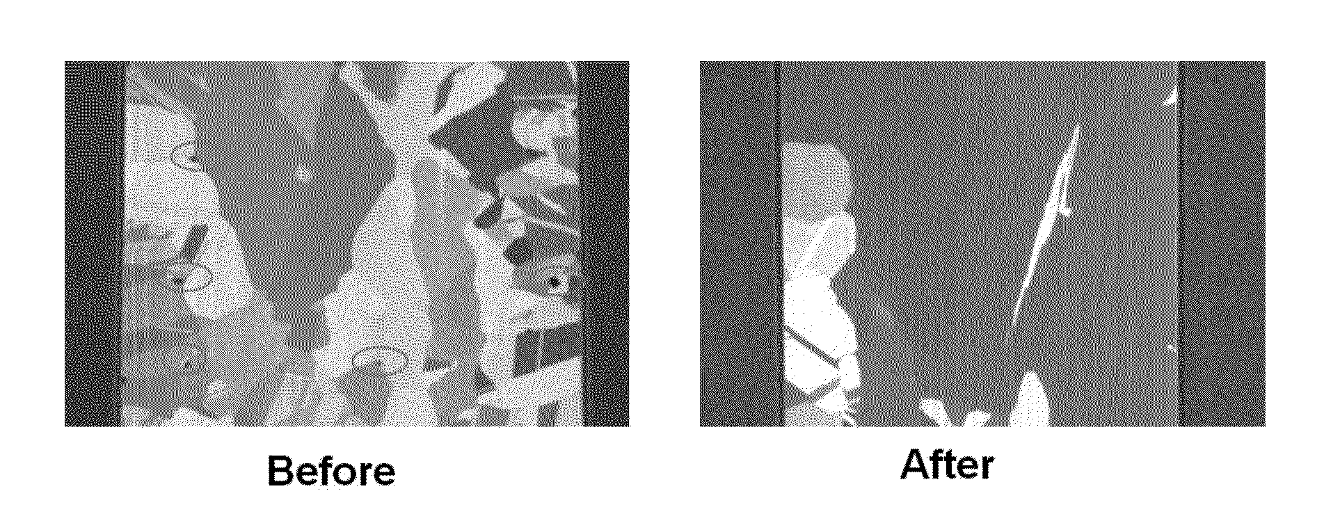
Additive for Reducing Voids after Annealing of Copper Plating with Through Silicon Via
a technology of copper plating and additives, which is applied in the field of additives for the copper plating process of through silicon via, can solve the problems of signal distortion and delay, and the possibility of micro-voids between different grains, and achieve the effects of simple formulation, rapid deposition speed, and easy operation
- Summary
- Abstract
- Description
- Claims
- Application Information
AI Technical Summary
Benefits of technology
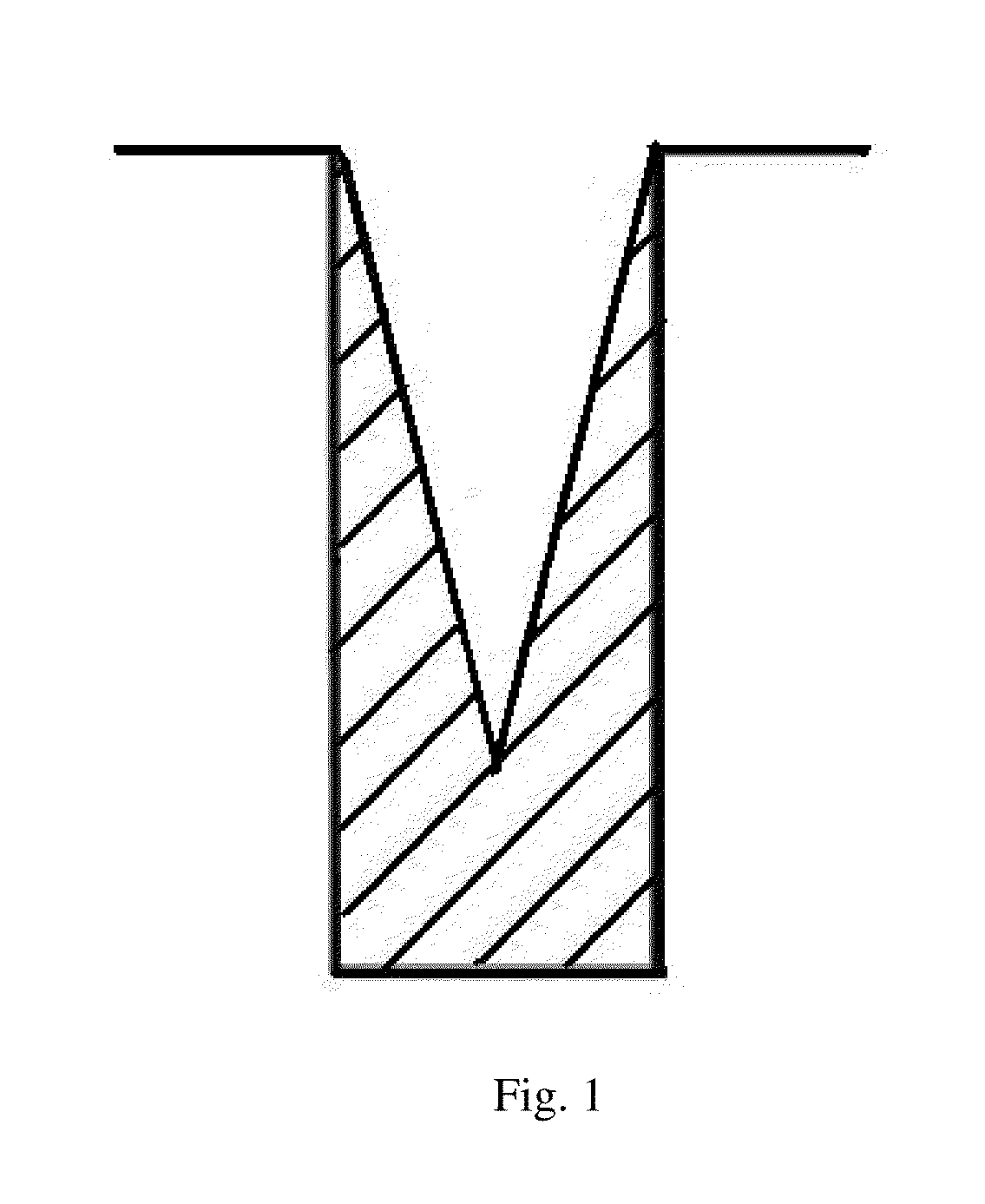
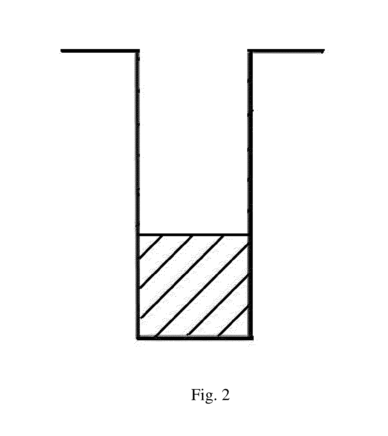
Problems solved by technology
Method used
Image

Examples
Embodiment Construction
[0022]The following illustration with figures will make a further description about the embodiments of this present invention.
[0023]The additive provided in the present invention for reducing voids after annealing of copper plating with TSV contains by weight percent: 0.05-1% of one or more of quaternized polyethylene imine and derivatives thereof having different molecular weights, and 1-10% of polyethylene glycol with an average molecular weight of 200-20000.
[0024]The general formula of the said quaternized polyethylene imine is:
according to the degree of polymerization of the polyethylene imine and the different quantities of the atoms N, the corresponding changes in the molecular weight is carried out.
[0025]The additive is used in combination with an electroplating solution of a copper methyl sulfonate system. The electroplating solution of a copper methyl sulfonate system contains 1-5 ml / L of additive by volume ratio.
[0026]The electroplating solution of a copper methyl sulfonat...
PUM
| Property | Measurement | Unit |
|---|---|---|
| volume ratio | aaaaa | aaaaa |
| volume ratio | aaaaa | aaaaa |
| volume ratio | aaaaa | aaaaa |
Abstract
Description
Claims
Application Information