Semiconductor Device and Electronic Device

a technology of semiconductor devices and electronic devices, applied in semiconductor devices, digital storage, instruments, etc., can solve the problems of data reliability decline, data is difficult to determine, data voltage increase to improve memory capacity is difficult to achieve, etc., to achieve high data reliability, large memory capacity, and small circuit area of memory cells

Active Publication Date: 2016-06-16
SEMICON ENERGY LAB CO LTD
View PDF1 Cites 9 Cited by
  • Summary
  • Abstract
  • Description
  • Claims
  • Application Information

AI Technical Summary

Benefits of technology

[0021]One embodiment of the present invention can provide a novel semiconductor device, a novel electronic device, or the like.
[0022]Another embodiment of the present invention can provide a semiconductor device or the like with a novel struc

Problems solved by technology

The structure in which the number of data voltages is increased to improve memory capacity is difficult to achieve because when the voltage levels read are varied due

Method used


Image

  • Semiconductor Device and Electronic Device
  • Semiconductor Device and Electronic Device
  • Semiconductor Device and Electronic Device

Examples


embodiment 1

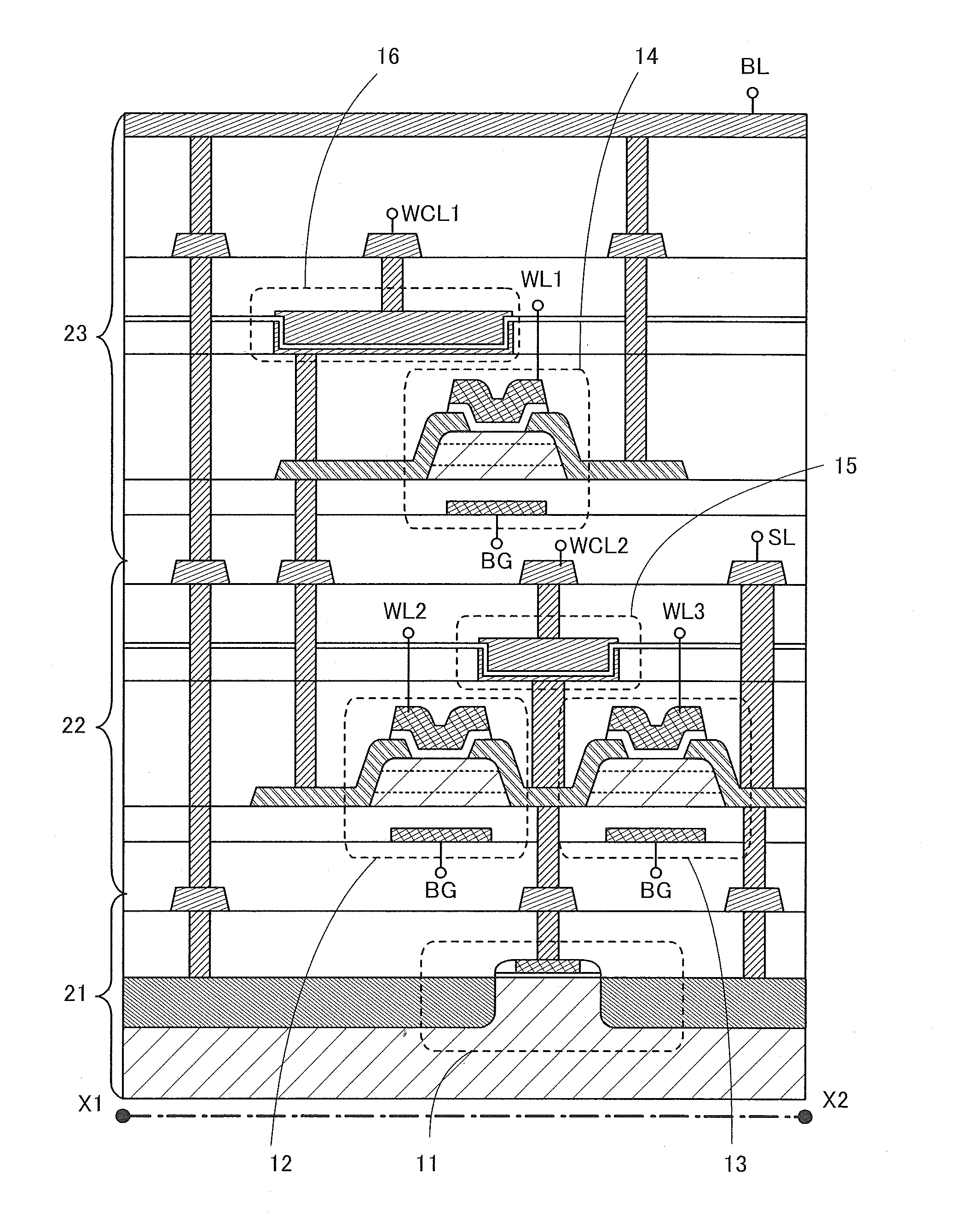
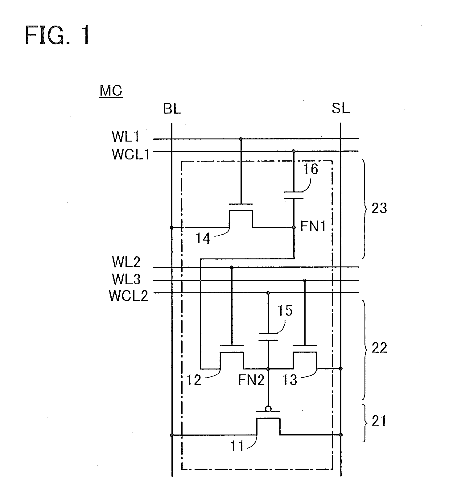
[0071]In this embodiment, a configuration of a memory cell included in a semiconductor device of one embodiment of the disclosed invention is described.

[0072]The memory cell described in this embodiment can retain multilevel data. The memory cell includes a plurality of data retention portions. The plurality of data retention portions each retain a plurality of voltage levels (data voltages) corresponding to multilevel data to increase memory capacity per memory cell. The data voltages are retained in such a manner that transistors having a low off-state current retain charges corresponding to the data voltages.

[0073]In the case where a memory cell including two data retention portions retains 8-bit data, for example, the two data retention portions each retain 4-bit data. In this case, each of the two data retention portions retains a data voltage corresponding to 4-bit data, i.e., 16 levels. The data voltage is converted, in accordance with the 16 levels, into the original data. A...

embodiment 2

[0141]In this embodiment, configurations of memory cells that are different from those in Embodiment 1 are described. Note that for the description of the same portions as those in Embodiment 1, Embodiment 1 is referred to, and the repeated description is omitted.

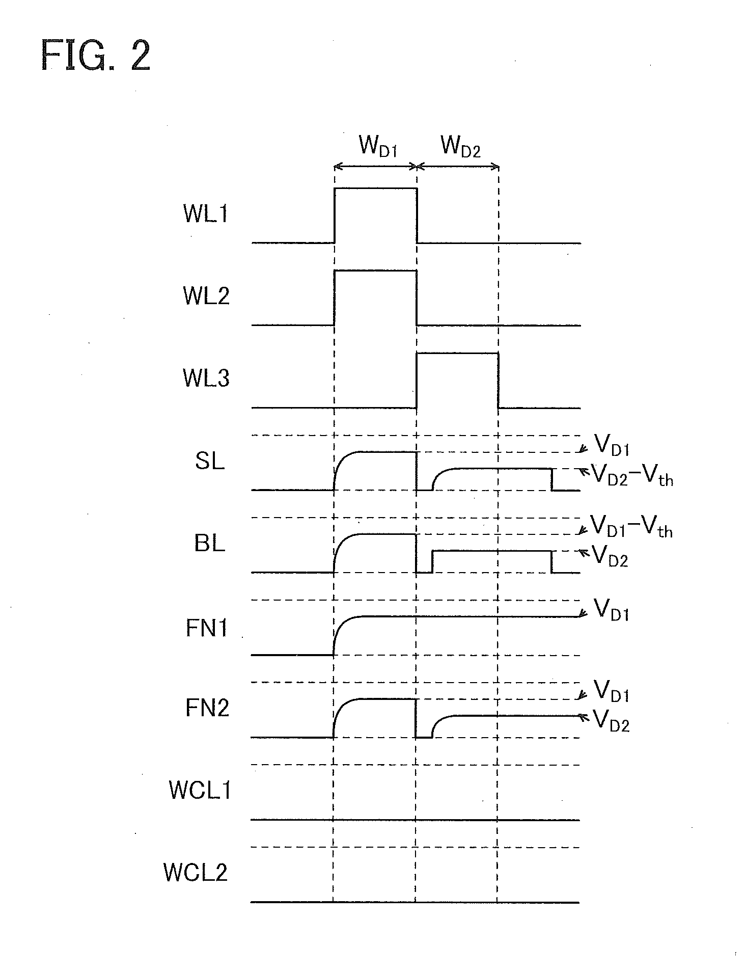
[0142]Specifically, a data voltage is written to a first data retention portion from a first wiring through a transistor for reading the data voltage, a second wiring, and a second data retention portion. A data voltage is written to the second data retention portion from the first wiring through a transistor for reading the data voltage and the second wiring. With such a configuration, writing the data voltage to the first data retention portion and writing the data voltage to the second data retention portion can be performed without meeting of the data voltages. Furthermore, the data voltage written to the data retention portion can be written as a data voltage (VD−Vth) obtained by subtracting a threshold voltage (Vth) o...

embodiment 3

[0188]In this embodiment, an example of a random access memory (RAM) including the memory cell illustrated in FIG. 1 is described. Description below is made with reference to FIG. 14, FIG. 15, FIG. 16, and FIG. 17. A RAM is referred to as a memory device or a semiconductor device in some cases.

[0189]FIG. 14 is a block diagram illustrating a configuration example of a RAM including the memory cell MC in FIG. 1.

[0190]A RAM 110 illustrated in FIG. 14 includes a memory cell array MCA including a plurality of memory cells MC in FIG. 1, a row decoder 111, a column decoder 112, and an A / D converter 113. In the RAM 110, the memory cells MC are arranged in a matrix of in rows and n columns (in and n are each a natural number of 2 or more).

[0191]In FIG. 14, wirings WL1[0] to WL1[m−1], wirings WCL1[0] to WCL1[m−1], wirings WL2[0] to WL2[m−1], wirings WL3[0] to WL3[m−1], wirings WCL2[0] to WCL2[m−1], wirings BL[0] to BL[n−1], and wirings SL[0] to SL[n−1] are provided.

[0192]In the memory cell ar...


PUM


Abstract

To provide a semiconductor device having large memory capacity and high reliability of data or a small-size semiconductor device having a small circuit area. A memory cell includes first and second data retention portions capable of storing multilevel data. A data voltage is written to the first data retention portion from a first wiring through a transistor for reading the data voltage and a second wiring, and a data voltage is written to the second data retention portion from the second wiring through a transistor for reading the data voltage and the first wiring. With the configuration, data voltages reduced by the threshold voltages of the transistors for reading the data voltage can be retained in the first and second data retention portions. The written data voltages where the threshold voltages of the transistors are canceled can be read by precharging and then discharging the first wiring.

Description

BACKGROUND OF THE INVENTION[0001]1. Field of the Invention[0002]One embodiment of the present invention relates to a semiconductor device and an electronic device.[0003]Note that one embodiment of the present invention is not limited to the above technical field. The technical field of the invention disclosed in this specification and the like relates to an object, a method, or a manufacturing method. In addition, one embodiment of the present invention relates to a process, a machine, manufacture, or a composition of matter. Specific examples of the technical field of one embodiment of the present invention disclosed in this specification include a semiconductor device, a display device, a light-emitting device, a power storage device, an imaging device, a memory device, a method for driving any of them, and a method for manufacturing any of them.[0004]In this specification and the like, a semiconductor device refers to an element, a circuit, a device, or the like that can function...

Claims


Application Information

Patent Timeline
IPC IPC(8): G11C5/00H01L29/786G11C11/24H01L29/16H01L27/12H01L27/115G11C5/06H01L29/24
CPCG11C5/005G11C5/06H01L29/7869G11C11/24H01L29/16H01L27/1207H01L27/115H01L29/24H01L27/0688H01L21/8258H10B12/00H10B41/70
Inventor MATSUZAKI, TAKANORIMIYAGUCHI, ATSUSHI
Owner SEMICON ENERGY LAB CO LTD
Why Eureka
Try Eureka