
Ultraviolet Reflective Rough Adhesive Contact

a technology of reflective contact and adhesive contact, which is applied in the manufacture of semiconductor/solid-state devices, semiconductor devices, electrical apparatus, etc., can solve the problems of resistive losses at the contact junction, low overall efficiency of these devices, and difficult to form good ohmic contact to the semiconductor layer, etc., to achieve good contact adhesion, increase light extraction efficiency, and low electrical resistance

Active Publication Date: 2016-06-16
SENSOR ELECTRONICS TECH
View PDF7 Cites 3 Cited by
  • Summary
  • Abstract
  • Description
  • Claims
  • Application Information

AI Technical Summary

Benefits of technology

The patent text describes a way to improve contacts between a semiconductor layer and a contact. This can increase the efficiency of light extraction in a DUV LED, while maintaining low electrical resistance and good contact adhesion.

Problems solved by technology

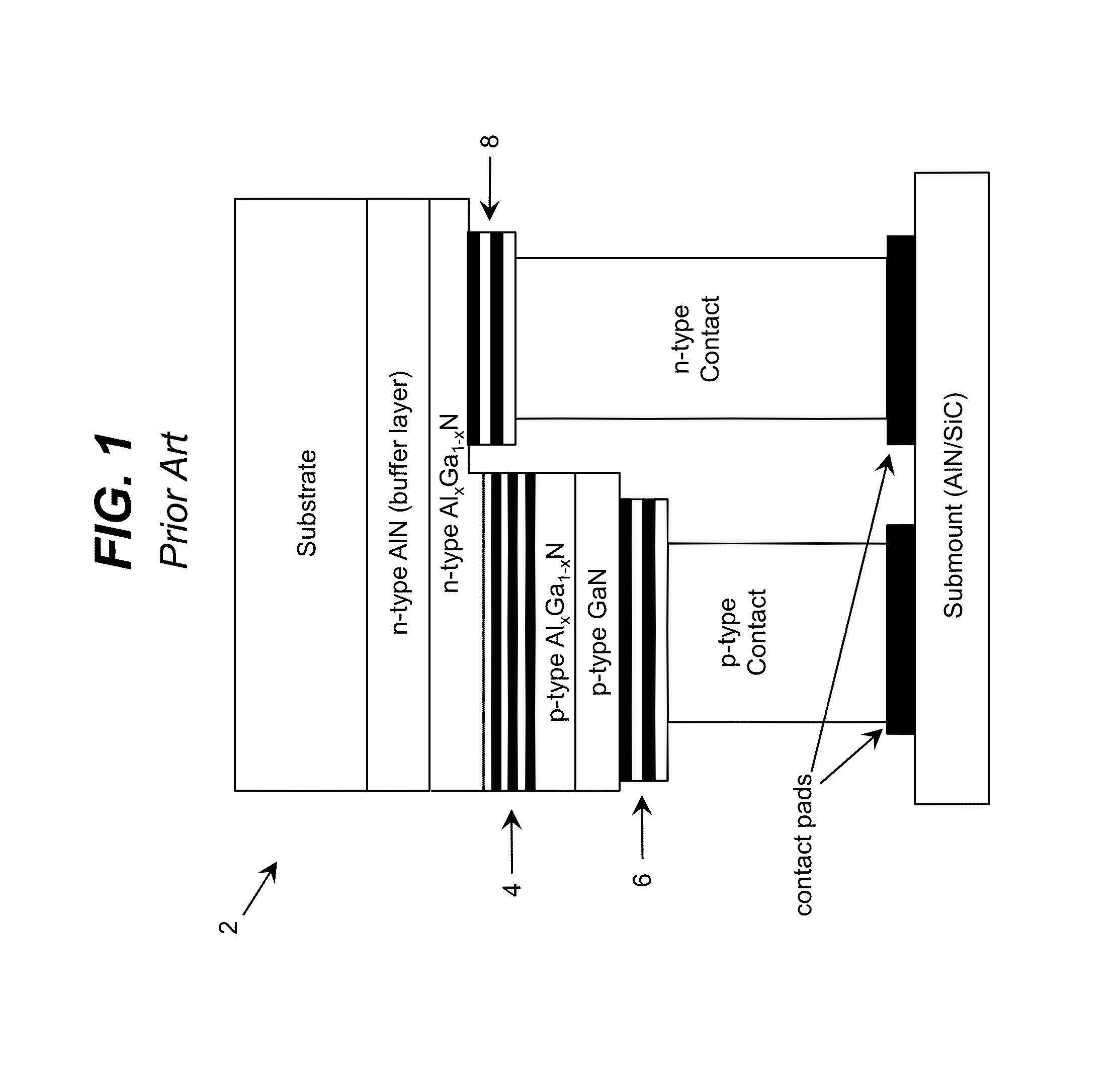
While there has been much advancement in improving the efficiency of DUV LEDs, the overall efficiency of these devices remains low.
The wide band-gap of group III nitride semiconductor materials makes it difficult to form a good ohmic contact to the semiconductor layers.
This can lead to resistive losses at the contact junction.
Aluminum is a good reflecting metal, however, aluminum does not produce ohmic contact and is unstable during packaging.

Method used


Image

  • Ultraviolet Reflective Rough Adhesive Contact
  • Ultraviolet Reflective Rough Adhesive Contact
  • Ultraviolet Reflective Rough Adhesive Contact

Examples


Embodiment Construction

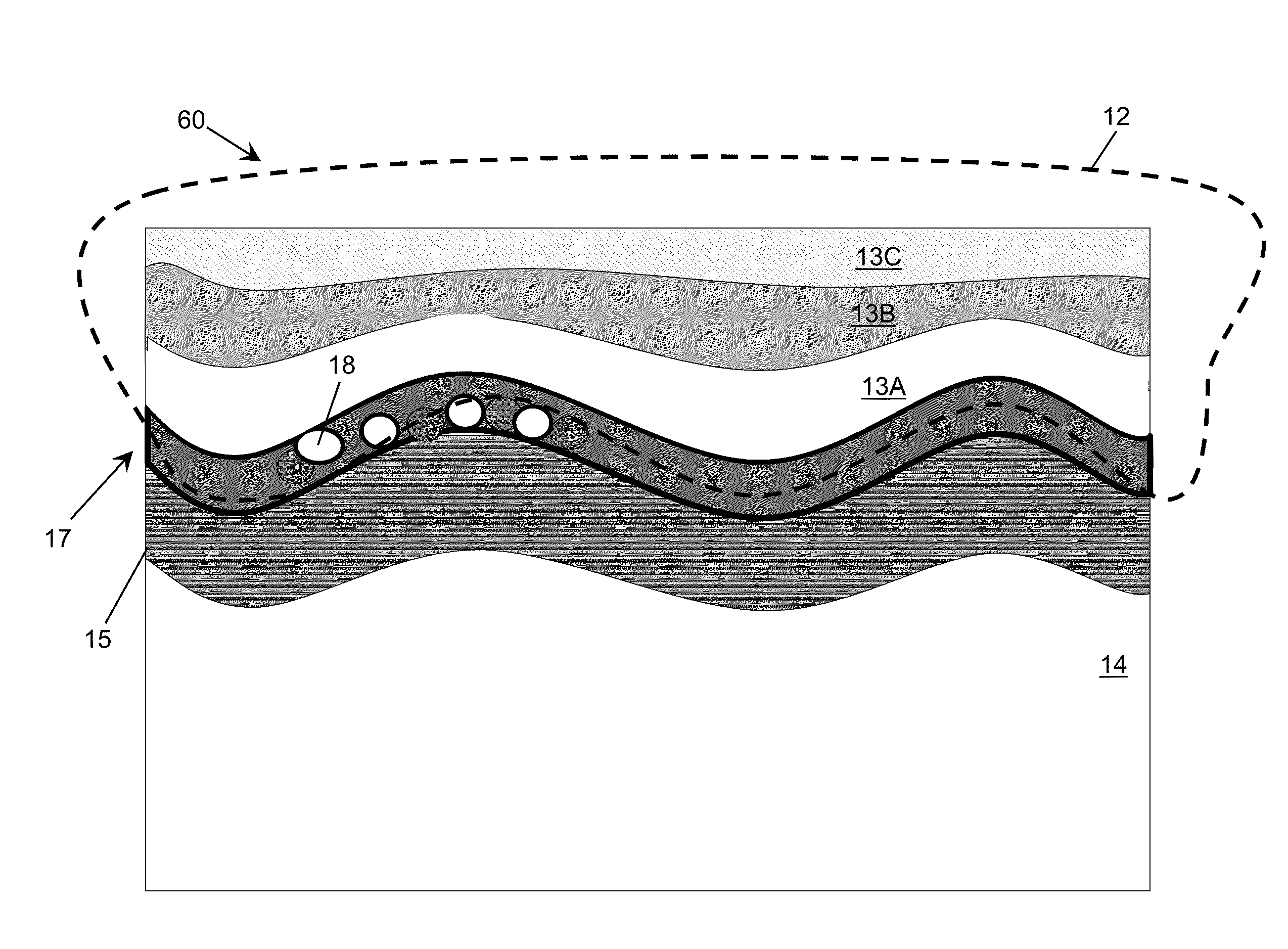
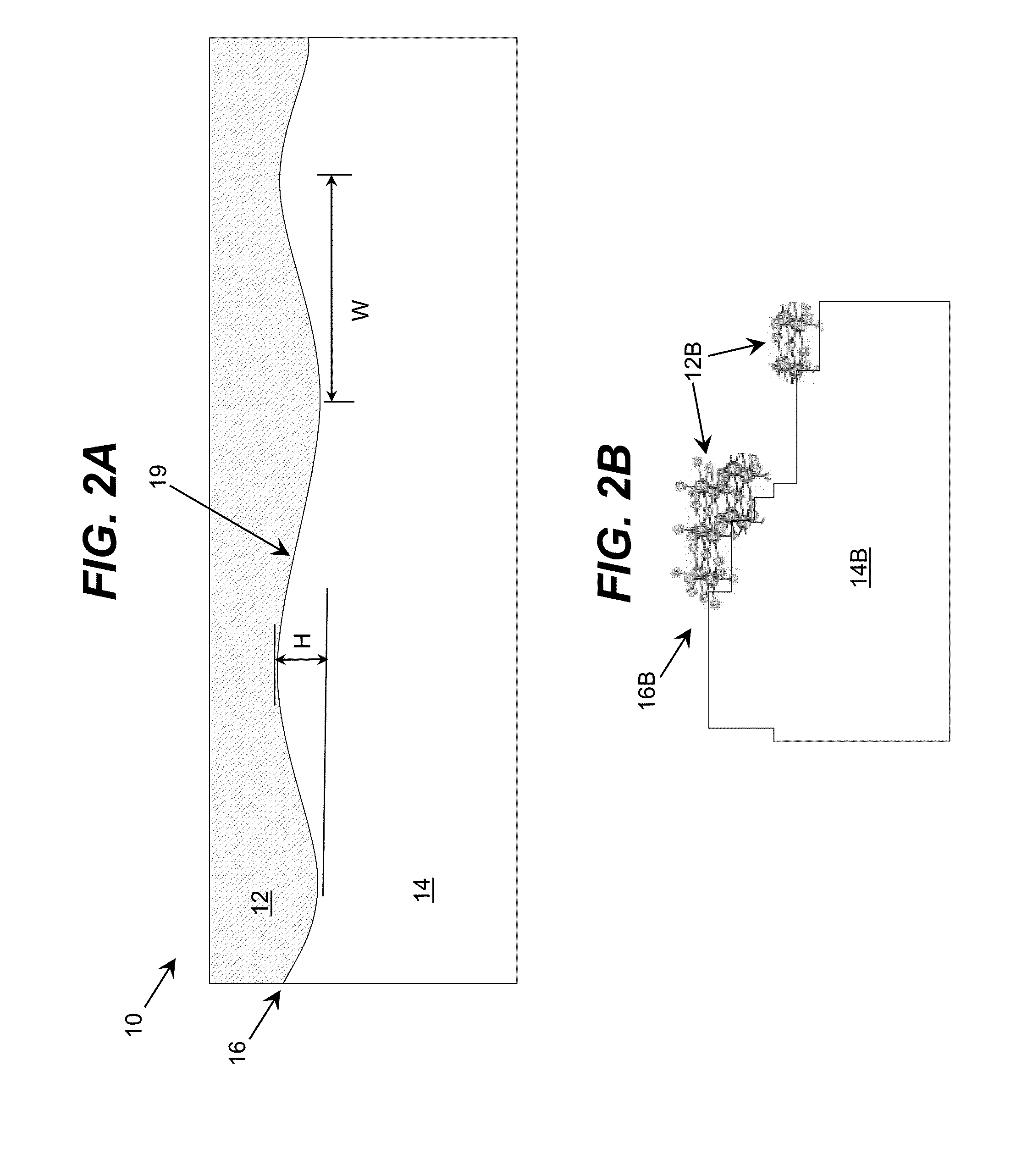
[0034]As indicated above, aspects of the invention provide a device including a first semiconductor layer and a contact to the first semiconductor layer. An interface between the first semiconductor layer and the contact includes a first roughness profile having a characteristic height and a characteristic width. The characteristic height can correspond to an average vertical distance between crests and adjacent valleys in the first roughness profile. The characteristic width can correspond to an average lateral distance between the crests and adjacent valleys in the first roughness profile. As used herein, unless otherwise noted, the term “set” means one or more (i.e., at least one) and the phrase “any solution” means any now known or later developed solution.

[0035]Furthermore, it is understood that a contact formed between two layers is considered “ohmic” or “conducting” when an overall resistance of the contact is no larger than the larger of the following two resistances: a cont...


PUM


Abstract

A device including a first semiconductor layer and a contact to the first semiconductor layer is disclosed. An interface between the first semiconductor layer and the contact includes a first roughness profile having a characteristic height and a characteristic width. The characteristic height can correspond to an average vertical distance between crests and adjacent valleys in the first roughness profile. The characteristic width can correspond to an average lateral distance between the crests and adjacent valleys in the first roughness profile.

Description

REFERENCE TO RELATED APPLICATIONS[0001]The current application is a continuation-in-part application of U.S. application Ser. No. 14 / 150,949, which was filed on 9 Jan. 2014, which claims the benefit of U.S. Provisional Application No. 61 / 750,452, titled “Ultraviolet Light Emitting Diode with Rough Reflective Adhesive Contact,” which was filed on 9 Jan. 2013, both of which are hereby incorporated by reference.TECHNICAL FIELD[0002]The disclosure relates generally to contacts for semiconductors, and more particularly, to an ultraviolet reflective rough adhesive contact.BACKGROUND ART[0003]Group III nitride semiconductors are widely used for efficient blue and ultraviolet light emitting diodes, lasers, ultraviolet detectors, and field effect transistors. Due to a wide band-gap, group III nitride semiconductor materials are one of the prime choices for deep ultraviolet light emitting diodes (DUV LEDs). While there has been much advancement in improving the efficiency of DUV LEDs, the ove...

Claims


Application Information

Patent Timeline
Patent Type & Authority Applications(United States)
IPC IPC(8): H01L33/40H01L33/32H01L33/22H01L33/00H01L33/06
CPCH01L33/405H01L33/007H01L33/0095H01L2933/0016H01L33/22H01L33/32H01L33/06H01L2924/12042H01L24/05H01L33/38H01L2224/0401H01L2224/06102H01L2224/1134H01L2924/12041H01L2224/16225H01L24/16H01L2924/00012H01L24/00H01L2924/00
Inventor GASKA, REMIGIJUSSHATALOV, MAXIM S.DOBRINSKY, ALEXANDERYANG, JINWEISHUR, MICHAELSIMIN, GRIGORY
Owner SENSOR ELECTRONICS TECH
Learn More