Package stucture and method of fabricating the same

a technology of packaging and routable regions, applied in the direction of electrical equipment, semiconductor devices, semiconductor/solid-state device details, etc., can solve the problems of poor yield, poor placement quality of semiconductor chips, and undesirably diminish the routable regions of inner wirings, so as to increase the routable region of the second wiring layer, reduce the overall size, and achieve the effect of increasing the routable region

Active Publication Date: 2016-06-23
PHOENIX PIONEER TECH
View PDF4 Cites 5 Cited by
  • Summary
  • Abstract
  • Description
  • Claims
  • Application Information

AI Technical Summary

Benefits of technology

[0026]In summary, according to the package structure of the present invention and the method of fabricating the same, two wiring layers are arranged in advance, then an opening is formed on the second insulating layer, so as to effectively utilize invalid regions outside the first conductors or second conductors to form the opening in 3D space, thereby reducing the overall size after packaging and increasing the routable region of the second wiring layer, as well as improving the electrical performance and signal stability.
[0027]Moreover, since the present invention does not utilize a core board, the overall size of the package substrate can be further reduced, thereby increasing routability.
[0028]In addition, according to the present invention, no stacking or laminating process is required to be performed on the substrate that already has an opening, and the electronic component is free of displacement due to any compression, as such, it is easier to align and fix the electronic component in position, thereby reducing yield loss.

Problems solved by technology

However, in the method of fabricating a package structure 1 according to the conventional art, the copper window 110 is used to serve as a spacing layer, which undesirably diminishes the routable regions for the inner wirings 11.
Moreover, an additional laser process with the use of CO2 laser to form the opening 130 increases the cost, and the organic glass fibers of core board 13 are exposed, which would result in poor yield and poor quality of the placement of the semiconductor chip 18.
In addition, with the use of PI tape as the carrier board 10 to fix the semiconductor chip 18 is also undesirable, which not only requires additional processes for attaching and detaching the tapes, additional cost involved for the tapes and other equipment is also undesirable.
As such, a pre-pressing and a curing pressing process are required, which not only is time consuming and expensive, it may also lead to dislocation (or even spinning) of the semiconductor chip 18, such that an accurate alignment for positioning the semiconductor chip 18 in the opening 130 is not easy, resulting in a poor alignment between the electrode pads 180 of the semiconductor chip 18 and the conductors 15.
Accordingly, poor electrical connection or electrical connection failure may occur and lead to a poor yield.
However, according to the conventional method of fabricating the package structure 1′, since the copper coil substrate is used to serve as the carrier board 10, delaminating may easily occur resulting in structural damages.
Also, a laser process is employed to make blind holes (i.e., at the corresponding positions of the conductors 15), such that only circular shaped openings could be made and the shapes of the openings are undesirable.
Further, as non-conductive material and dispensing method are used to attach the passive component 18′, and the diameter of the dispensed particle is more than 200 μm, the dispensed adhesive in each dispensing process varies greatly in size of the diameter and is difficult to be controlled, causing the adhesive 180′ to easily spread to other regions, thus contaminating the wirings of the first wiring layer 11′ thereby resulting in poor reliability.
As such, the first dielectric layer 13′ and the second dielectric layer can easily be dislocated, thereby increasing the fabricating time and cost.
Moreover, after placing the passive component 18′ and before curing the dielectric encapsulating layer 16′, the passive component 18′ is not fixed yet, and can easily dislocate, resulting in a poor yield.
In addition, with the use of the conductors 15 to establish an electrical connection path to one side of the passive component 18′, the electrical path is increased as well as the risk of signal loss is raised, and thus the cost of using unconventional MLCC as the passive component 18′ is significantly high.

Method used


Image

  • Package stucture and method of fabricating the same
  • Package stucture and method of fabricating the same
  • Package stucture and method of fabricating the same

Examples


Embodiment Construction

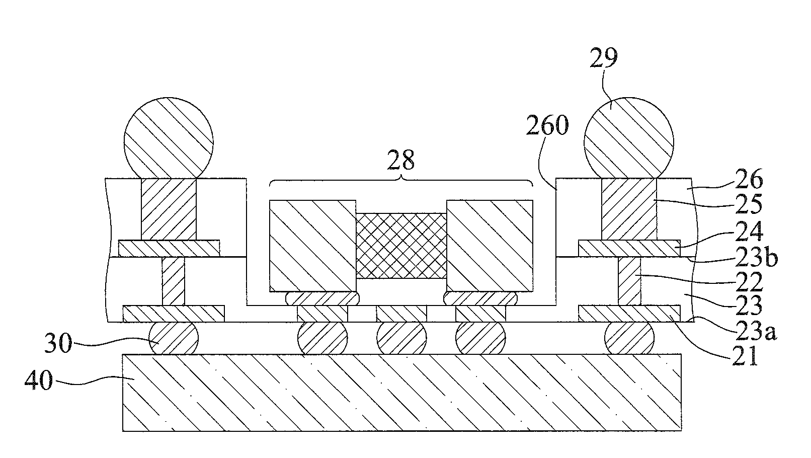
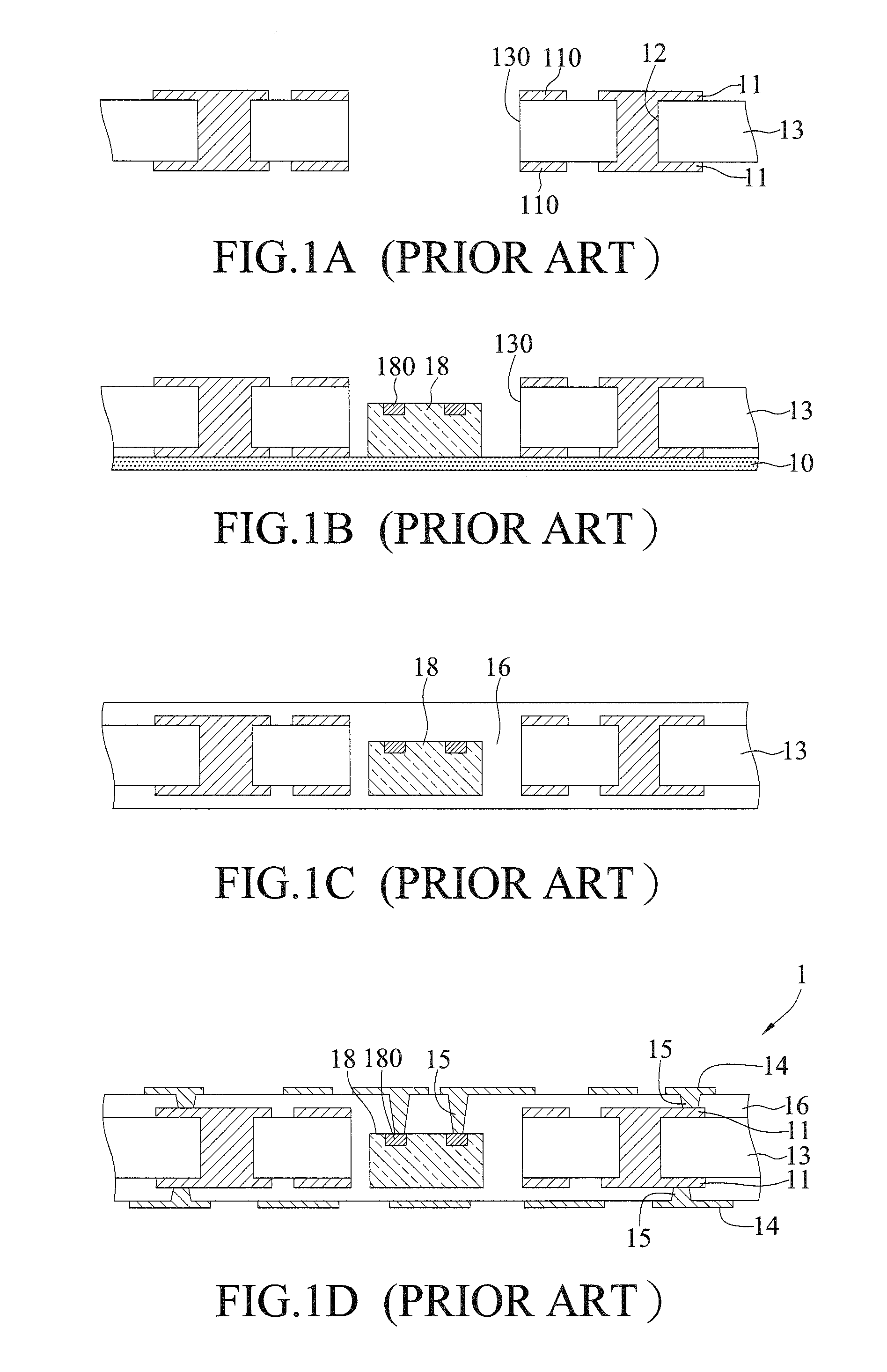
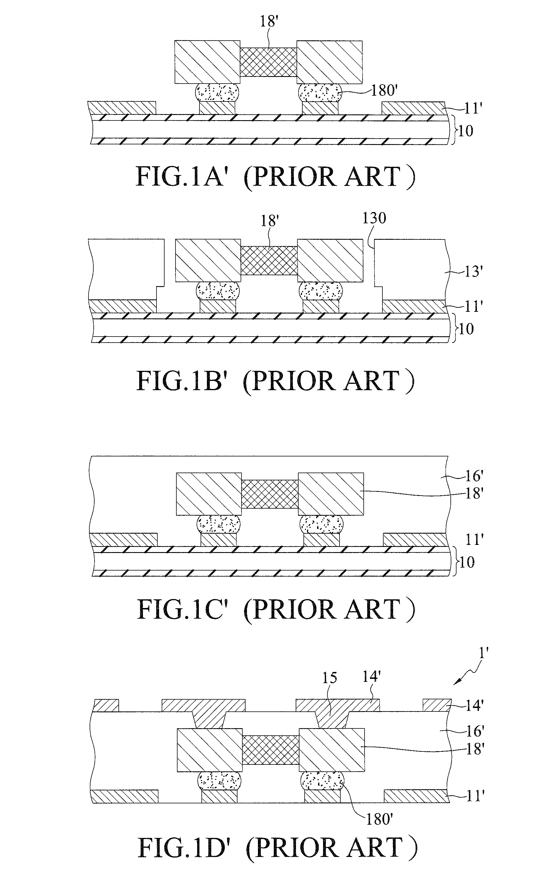
[0032]The present invention is described in the following with specific embodiments, so that one skilled in the pertinent art can easily understand other advantages and effects of the present invention from the disclosure of the present invention.

[0033]It should be advised that the structure, ratio, and size as illustrated in this context are only used for disclosures of this specification, provided for persons skilled in the art to understand and read, and technically do not have substantial meaning. Any modification of the structure, change of the ratio relation, or adjustment of the size should be involved in the scope of disclosures in this specification without influencing the producible efficacy and the achievable objective of this specification. Further, terms such as “top”, “bottom”, “first”, “second” and “one” are merely for illustrative purpose and should not be construed to limit the scope of the present invention. Those changes or adjustments of relative relationship wit...


PUM


Abstract

A package structure and a method of fabricating the same are provided. The method includes forming a first wiring layer on a carrier board, forming a plurality of first conductors on the first wiring layer, encapsulating the first wiring layer and the first conductors with a first insulating layer, forming a second wiring layer on the first insulating layer, forming a plurality of second conductors on the second wiring layer, encapsulating the second wiring layer and the second conductors with a second insulating layer, and forming at least one opening in the second insulating layer. The at least one opening extends to a second surface of the first insulating layer, such that at least one electronic component can be disposed in the at least one opening. With forming two insulating layers first followed by forming the at least one opening, there is no need to stack or laminate the substrate that already has an opening, and the electronic component is free of displacement due to any compression. Therefore, a package structure thus fabricated has an increased yield rate.

Description

BACKGROUND OF THE INVENTION[0001]1. Field of the Invention[0002]The present invention relates to package structures, and, more particularly, to a package structure with embedded electronic components and a method of fabricating the same.[0003]2. Description of Related Art[0004]As the packaging technology advances, semiconductor devices with different types of chip packaging technologies have been developed to be incorporated in various different electronic devices such as smart phones, tablets, networks, or laptops. Such semiconductor device mainly involves disposing a chip on a package substrate, where the chip is electrically connected with the package substrate, followed by an encapsulating process with the use of an encapsulating material. In order to reduce the package height, a type of package with the chip embedded in a package substrate is preferred, as the overall package size is reduced while the electrical performance is improved.[0005]FIGS. 1A-1D are cross-sectional view...

Claims


Application Information

Patent Timeline
Patent Type & Authority Applications(United States)
IPC IPC(8): H01L23/498H01L21/48
CPCH01L23/49838H01L21/4857H01L23/49816H01L23/49822H01L21/4853H01L23/5389H01L2924/0002Y02P80/30
Inventor HSU, SHIH-PINGTSENG, CHAO-CHUNG
Owner PHOENIX PIONEER TECH
Why Eureka
Try Eureka