Epitaxial structure and growth thereof
- Summary
- Abstract
- Description
- Claims
- Application Information
AI Technical Summary
Benefits of technology
Problems solved by technology
Method used
Image

Examples
Embodiment Construction
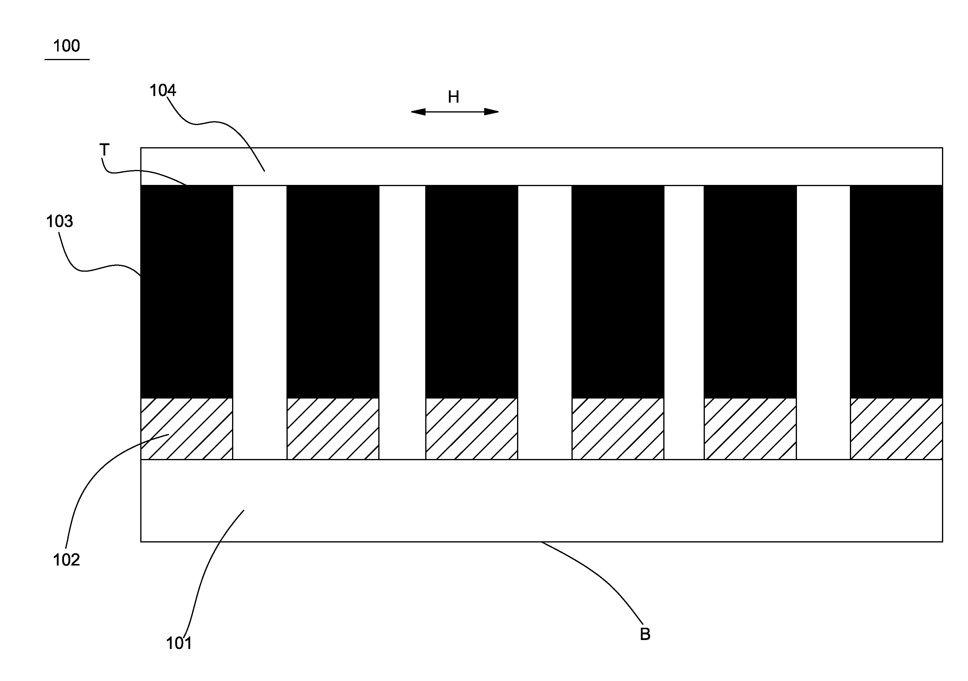
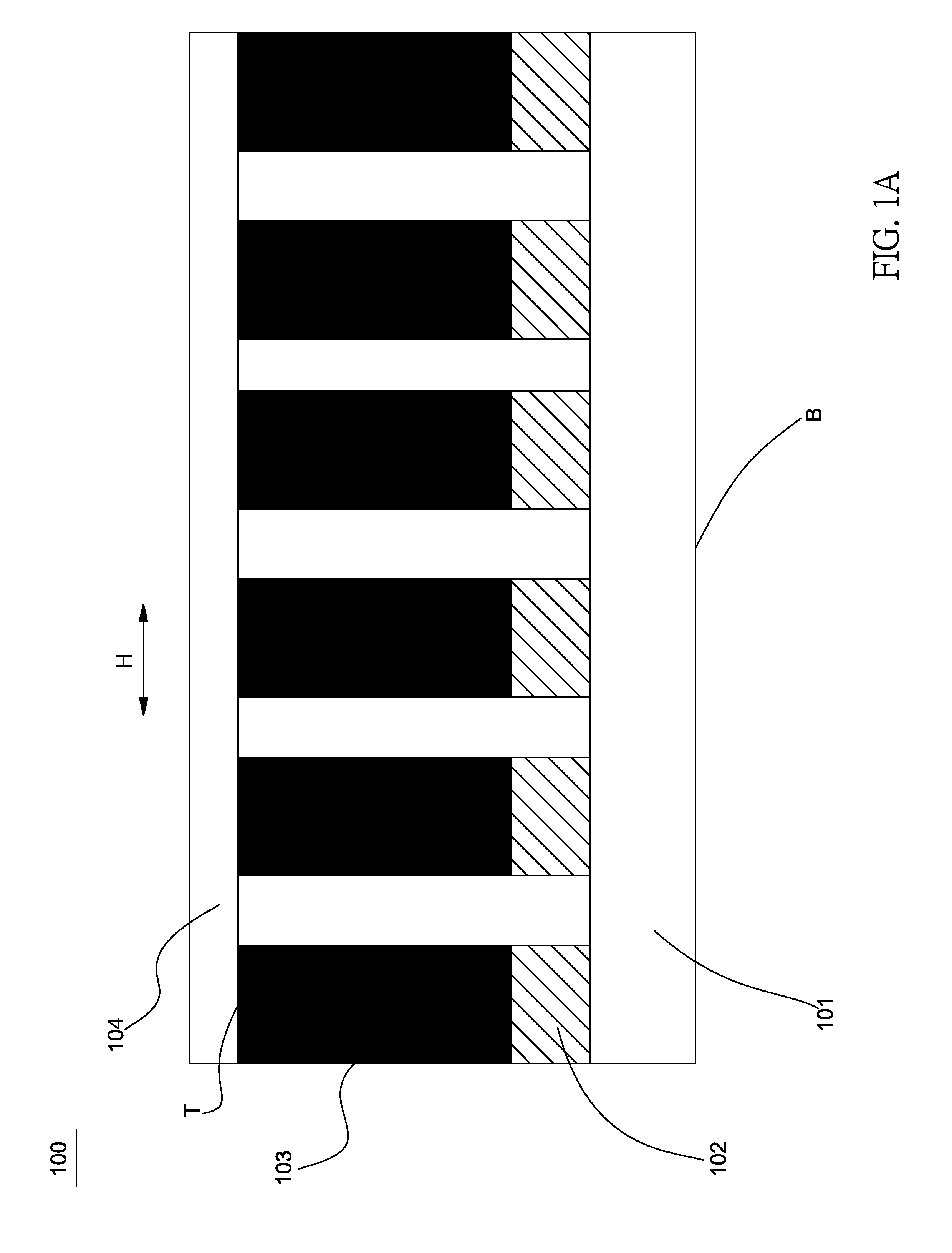
[0017]FIG. 1A is a schematic view showing an epitaxial growth structure of the invention. Referring to FIG. 1A, the structure of this embodiment is a GaN epitaxial growth structure, and the epitaxial growth structure 100 comprises a substrate 101, a plurality of seeds 102, a plurality of nanorods 103 and a film 104.
[0018]It is to be noted that the substrate 101 in this embodiment is implemented by a silicon (Si) substrate, a sapphire substrate, a gallium nitride substrate or a silicon carbide substrate.
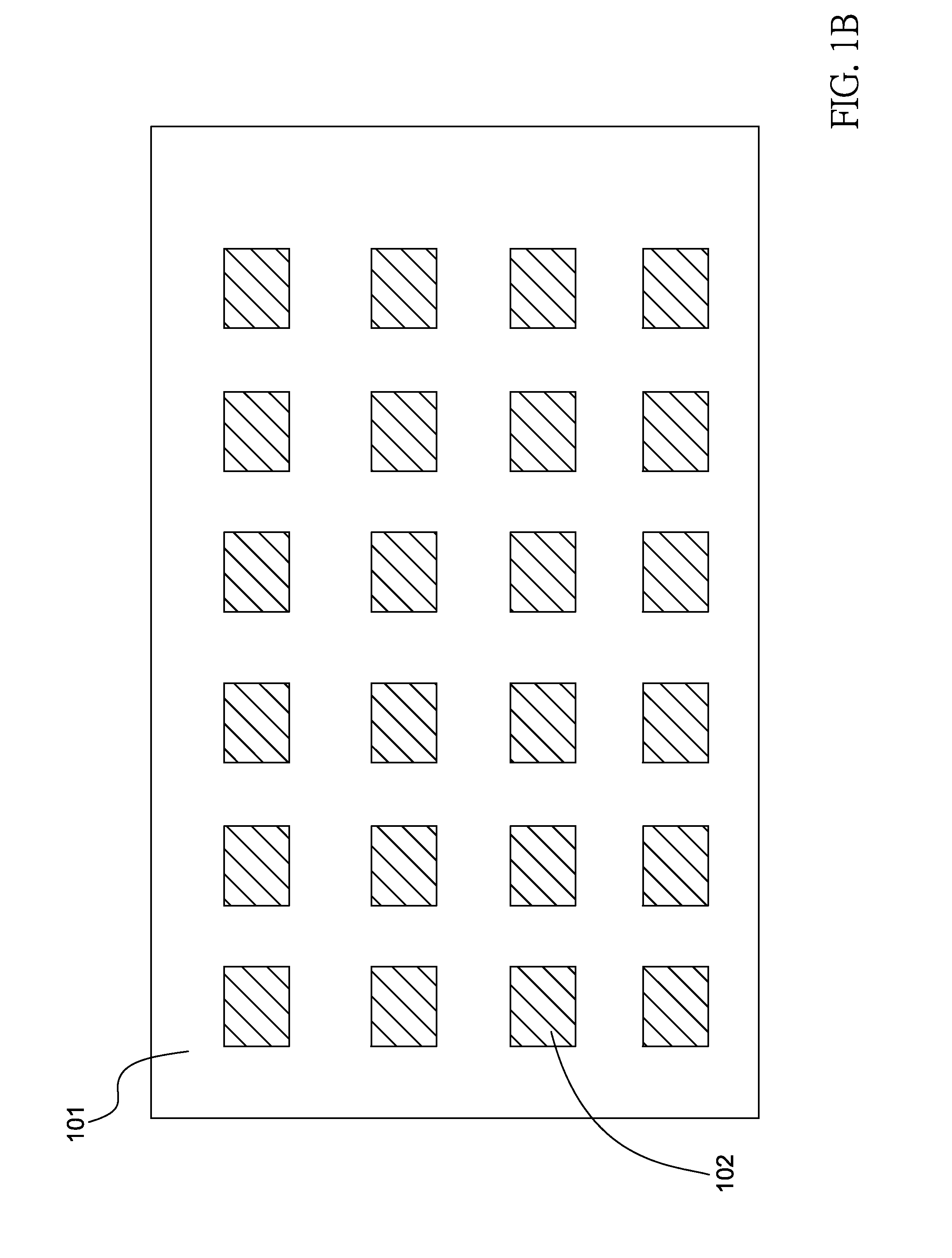
[0019]The substrate 101 is disposed on a bottom layer B of the epitaxial growth structure 100. Next, seeds 102 are arranged in an array and disposed on a surface of the substrate 101. FIG. 1B is a schematic top view showing the substrate 101 and the seeds 102 of the epitaxial growth structure of the invention. Referring to FIGS. 1A and 1B, the seeds 102 have regular gaps in this embodiment.
[0020]FIG. 1C is a schematic top view showing the substrate and nanorods of the epitaxial growth...
PUM
 Abstract
Description
Claims
Application Information
 - R&D
- Intellectual Property
- Life Sciences
- Materials
- Tech Scout
- Unparalleled Data Quality
- Higher Quality Content
- 60% Fewer Hallucinations
Browse by: Latest US Patents, China's latest patents, Technical Efficacy Thesaurus, Application Domain, Technology Topic, Popular Technical Reports.
© 2025 PatSnap. All rights reserved.Legal|Privacy policy|Modern Slavery Act Transparency Statement|Sitemap|About US| Contact US: help@patsnap.com