

Hetero-junction solar cell and manufacturing method thereof
- Summary
- Abstract
- Description
- Claims
- Application Information
AI Technical Summary
Benefits of technology
Problems solved by technology
Method used
Image

Examples
Embodiment Construction
[0028]The invention disclosed herein is directed to a hetero junction solar cell and a manufacturing method thereof. In the following description, numerous details are set forth in order to provide a thorough understanding of the present invention. It will be appreciated by one skilled in the art that variations of these specific details are possible while still achieving the results of the present invention. In other instance, well-known components are not described in detail in order not to unnecessarily obscure the present invention.
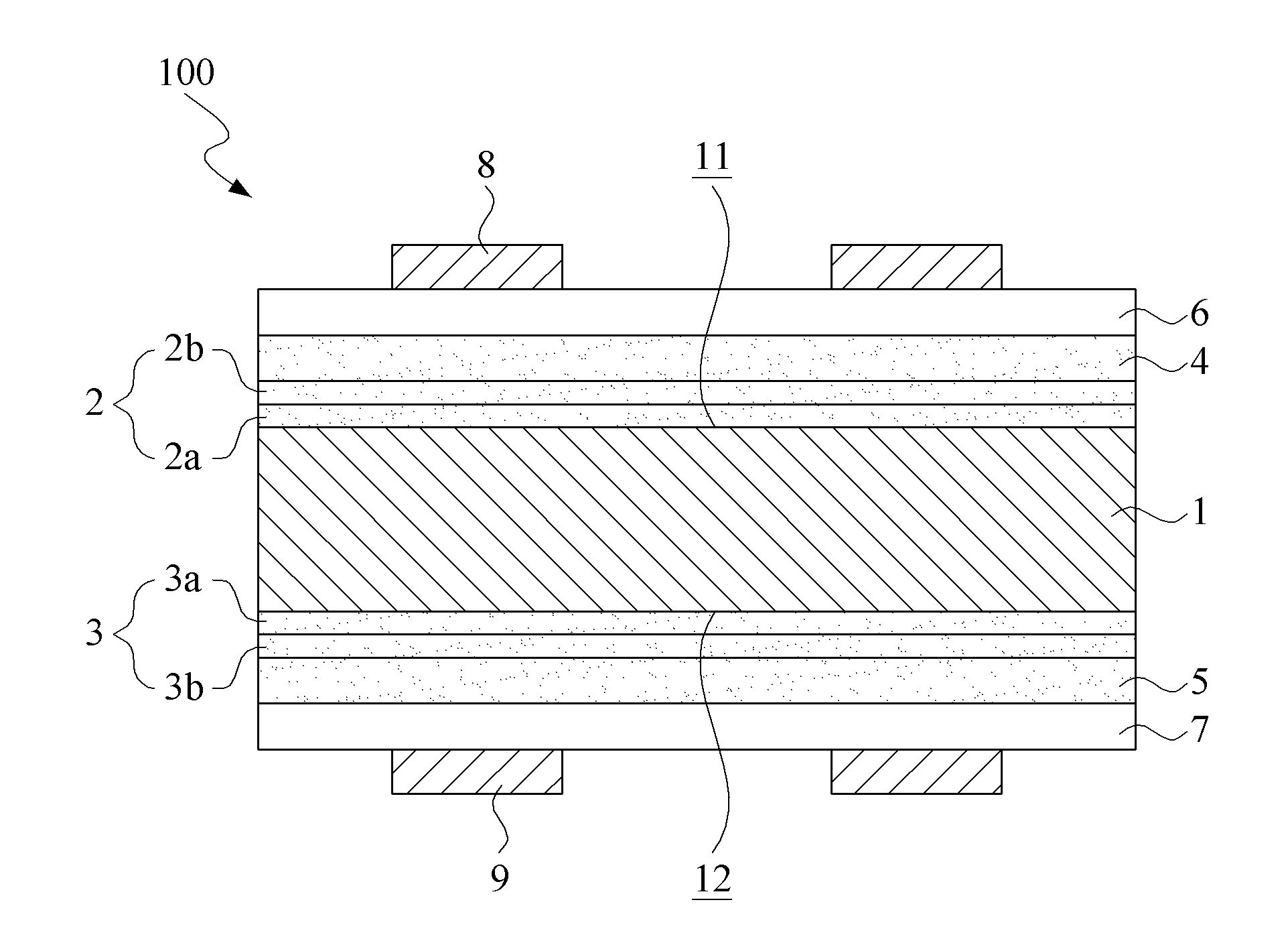
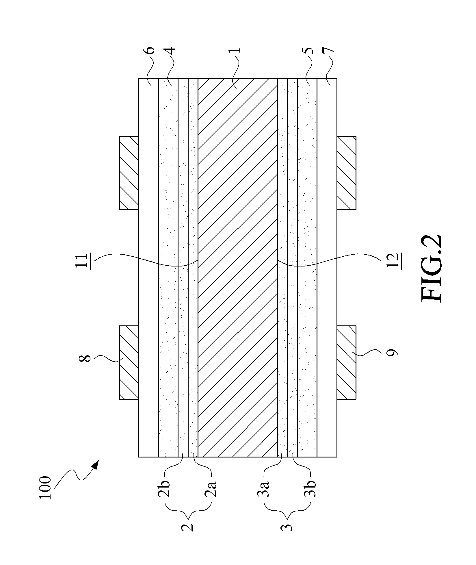
[0029]Referring to FIG. 2, a schematic view of the preferred hetero junction solar cell in accordance with the present invention is shown. As shown, the hetero junction solar cell 100 includes a semiconductor substrate 1, a first n-type buffer layer 2, a second n-type buffer layer 3, a first amorphous silicon layer 4, a second amorphous silicon layer 5, a first TCO layer 6, a second TCO layer 7, a plurality of first leads 8 and a plurality of second l...
PUM
 Abstract
Description
Claims
Application Information