Method and apparatus for anisotropic tungsten etching

a technology of anisotropic tungsten and tungsten, which is applied in the direction of electrical equipment, basic electric elements, electric discharge tubes, etc., can solve the problem of limited methods of tungsten etching

Active Publication Date: 2016-07-07
LAM RES CORP
View PDF3 Cites 97 Cited by
  • Summary
  • Abstract
  • Description
  • Claims
  • Application Information

AI Technical Summary

Benefits of technology

[0011]In one implementation the semiconductor substrate comprises a recessed feature comprising an exposed layer of tungsten-containing material at the bottom of the recessed feature. The etching can remove the tungsten-containing material from the bottom of the recessed feature without substantially altering the width or diameter of the recessed feature. In some embodiments the width or diameter of the recessed feature is less than about 150 nm.

Problems solved by technology

While there is a variety of methods that can be used for tungsten deposition, including chemical vapor deposition (CVD), atomic layer deposition (ALD), and physical vapor deposition (PVD), the methods for tungsten etching are still limited.

Method used


Image

  • Method and apparatus for anisotropic tungsten etching
  • Method and apparatus for anisotropic tungsten etching
  • Method and apparatus for anisotropic tungsten etching

Examples


example

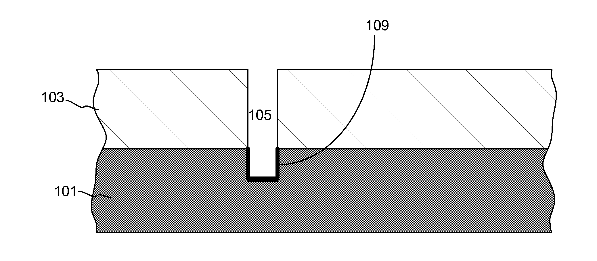
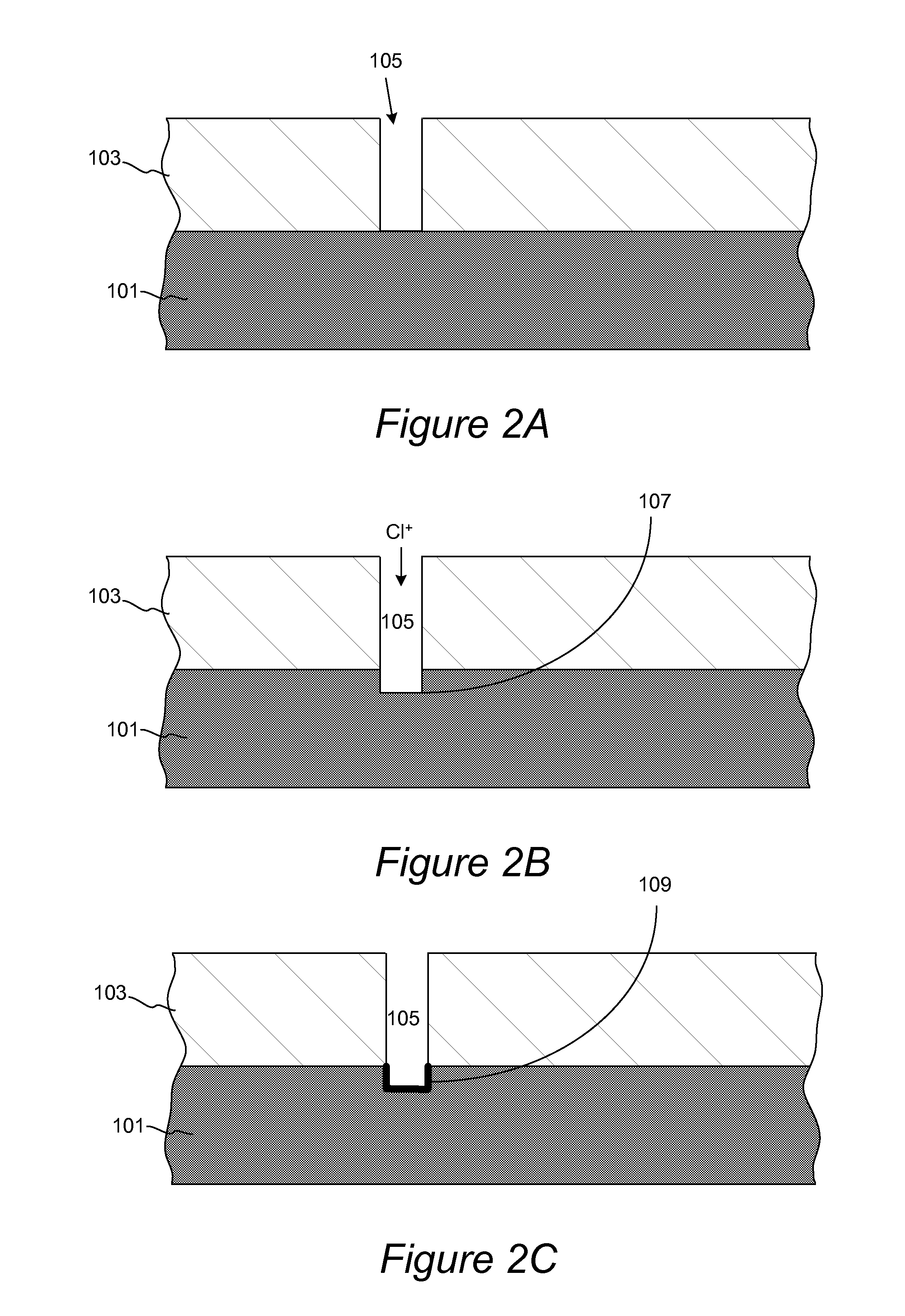
[0052]In an experimentally validated example a substrate including an array or matrix of recessed features was provided. The recessed features had an aspect ratio of 10:1 and width of 27 nm. The recessed features were made in a silicon oxide material and had an exposed layer of tungsten at the bottom of recessed features. Tungsten was etched in the Kiyo FX apparatus available from Lam Research Corporation. The substrate was placed into the process chamber and Cl2 was provided to the process chamber at a flow rate of 100 sccm. The plasma was formed by providing a power of 300 W to the 13.56 MHz ICP excitation source, and by providing a 1500 V RF bias to the substrate holding chuck. The bias was applied in pulses with a 10% duty cycle. The timing diagram for bias pulsing is schematically illustrated in FIG. 4. The substrate was treated with Cl2 in a plasma for 12 seconds at a pressure of 5 mTorr and a temperature of 70° C. (referring to a temperature at the substrate holder). Next, th...


PUM

PropertyMeasurementUnit
diameteraaaaaaaaaa
thicknessaaaaaaaaaa
widthsaaaaaaaaaa

Abstract

Methods for anisotropically etching a tungsten-containing material (such as doped or undoped tungsten metal) include cyclic treatment of tungsten surface with Cl2 plasma and with oxygen-containing radicals. Treatment with chlorine plasma is performed while the substrate is electrically biased resulting in predominant etching of horizontal surfaces on the substrate. Treatment with oxygen-containing radicals passivates the surface of the substrate to etching, and protects the vertical surfaces of the substrate, such as sidewalls of recessed features, from etching. Treatment with Cl2 plasma and with oxygen-containing radicals can be repeated in order to remove a desired amount of material. Anisotropic etching can be performed selectively in a presence of dielectric materials such as silicon oxide, silicon nitride, and silicon oxynitride.

Description

FIELD OF THE INVENTION[0001]The present invention pertains to methods of removing layers of material on a substrate. The methods are particularly useful for anisotropic removal of tungsten-containing material on a semiconductor substrate.BACKGROUND OF THE INVENTION[0002]Fabrication of integrated circuits (IC) on semiconductor substrates involves deposition and etching of multiple layers of materials in order to form a desired pattern of conductive paths in a layer of dielectric. Anisotropic etching (i.e. predominant etching in a selected direction) is a valuable tool for forming recessed features on semiconductor substrates. In a typical example of anisotropic etching, the material is etched out in a vertical direction, without horizontal etching. For example, the material can be removed from the bottom of a recessed feature, while preserving the width of the recessed feature.[0003]Tungsten and tungsten-containing materials emerge as materials that find many uses in IC fabrication, ...

Claims


Application Information

Patent Timeline
Patent Type & Authority Applications(United States)
IPC IPC(8): H01L21/3213H01L21/027H01L21/67
CPCH01L21/32136H01L21/0274H01L21/67069H01J37/32H01J37/3244H01L21/3213H01J37/32449H01J2237/334H01L21/32138H01L21/32139
Inventor TAN, ZHONGKUIFU, QIANHSIAO, HUAI-YU
Owner LAM RES CORP
Why Eureka
Try Eureka