Semiconductor device and formation method thereof

a semiconductor and semiconductor technology, applied in the field of semiconductor technology, can solve the problems of resistors not being in sufficient contact with conductive plugs, increasing chip production costs,

Active Publication Date: 2016-07-14
SEMICON MFG INT (SHANGHAI) CORP
View PDF5 Cites 21 Cited by
  • Summary
  • Abstract
  • Description
  • Claims
  • Application Information

AI Technical Summary

Problems solved by technology

However, due to the difficulty in accurately controlling the polysilicon resistance and specific doping process required by the polysilicon, the production cost of the chip increases.
Such resistors, however, may not be in sufficient contact with conductive plugs.

Method used


Image

  • Semiconductor device and formation method thereof
  • Semiconductor device and formation method thereof
  • Semiconductor device and formation method thereof

Examples


Embodiment Construction

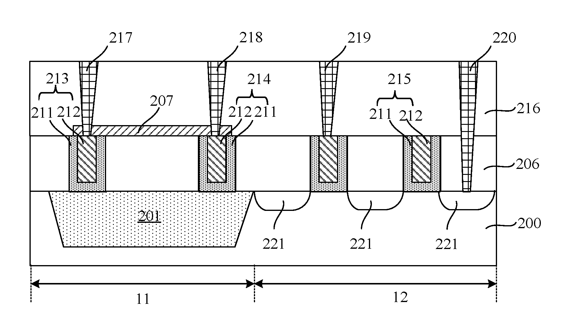
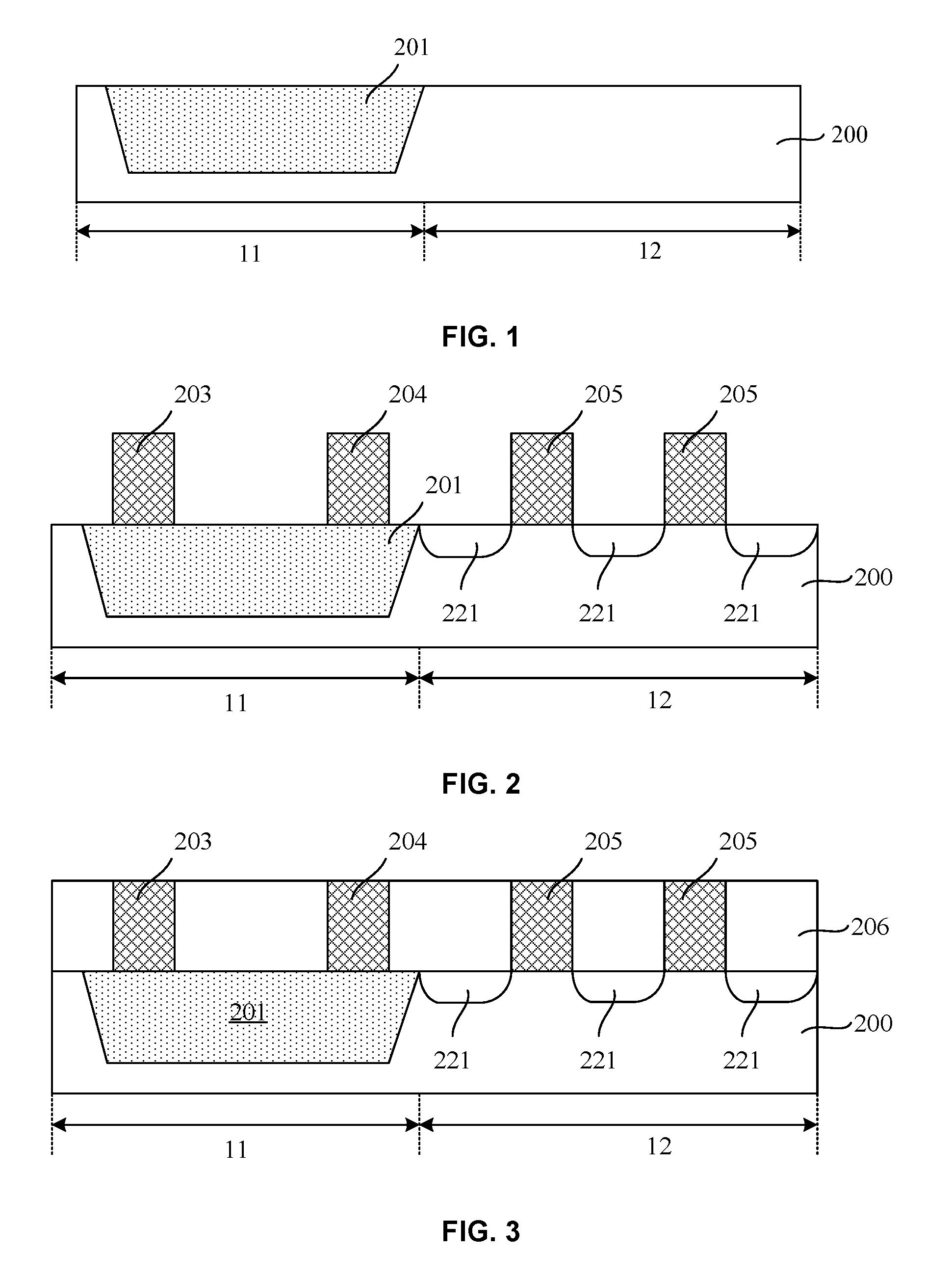
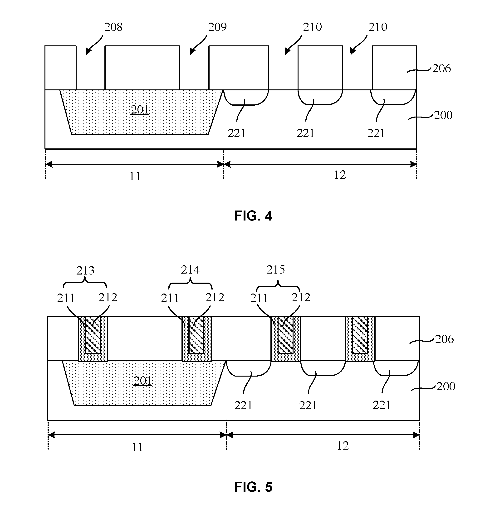
[0016]Reference will now be made in detail to exemplary embodiments of the invention, which are illustrated in the accompanying drawings. Hereinafter, embodiments consistent with the disclosure will be described with reference to drawings. Wherever possible, the same reference numbers will be used throughout the drawings to refer to the same or like parts. It is apparent that the described embodiments are some but not all of the embodiments of the present invention. Based on the disclosed embodiments, persons of ordinary skill in the art may derive other embodiments consistent with the present disclosure, all of which are within the scope of the present invention.

[0017]Resistors formed using a metal nitride material may not be in sufficient contact with plugs or conductive plugs. The disclosed methods and semiconductor devices are directed to solve the problem set forth above or other problems in the art.

[0018]To form a metal nitride resistor, a semiconductor substrate may be provid...


PUM


Abstract

The present disclosure provides a semiconductor device and formation method thereof. A shallow trench isolation structure is formed in a semiconductor substrate. A first dielectric layer is formed on the semiconductor substrate. First and second dummy gate structures are formed on the shallow trench isolation structure and through the first dielectric layer. A resistive material layer is formed on the first and second dummy gate structures and on the first dielectric layer between the first and second dummy gate structures. A second dielectric layer is formed on the first dielectric layer and the resistive material layer. A first plug is formed in the second dielectric layer and the resistive material layer and on the first dummy gate structure. A second plug is formed in the second dielectric layer and the resistive material layer and on the second dummy gate structure.

Description

CROSS-REFERENCES TO RELATED APPLICATIONS[0001]This application claims the priority of Chinese patent application No. CN201510009320.8, filed on Jan. 8, 2015, the entire content of which is incorporated herein by reference.FIELD OF THE DISCLOSURE[0002]The present disclosure relates to the field of semiconductor technology and, more particularly, relates to a semiconductor device and formation method thereof.BACKGROUND[0003]The semiconductor integrated circuit is widely used in various electronic products, such as: cell phones, computers, personal gaming devices, and navigation devices. The semiconductor integrated circuit is formed using a semiconductor fabrication process, for example, to fabricate various transistors, resistors, capacitors and other components on a wafer, and to interconnect the components through multilayered wirings to form a complete electronic circuit.[0004]Particularly in the integrated circuits for analog circuits and high voltage cables, a large number of re...

Claims


Application Information

Patent Timeline
Patent Type & Authority Applications(United States)
IPC IPC(8): H01L27/06H01L23/535H01L29/49H01L29/06H01L29/66H01L21/8238H01L27/092H01L49/02
CPCH01L27/0629H01L27/0924H01L23/535H01L28/24H01L29/0653H01L29/4966H01L21/823821H01L21/823871H01L21/823878H01L21/823842H01L29/66545H01L23/485H01L23/5228H01L2924/0002H01L29/517H01L29/66795H01L29/785H01L2924/00
Inventor ZHANG, BUXINTSAI, MENGFENG
Owner SEMICON MFG INT (SHANGHAI) CORP
Why Eureka
Try Eureka