

Method of manufacturing semiconductor device
- Summary
- Abstract
- Description
- Claims
- Application Information
AI Technical Summary
Benefits of technology
Problems solved by technology
Method used
Image

Examples
first embodiment
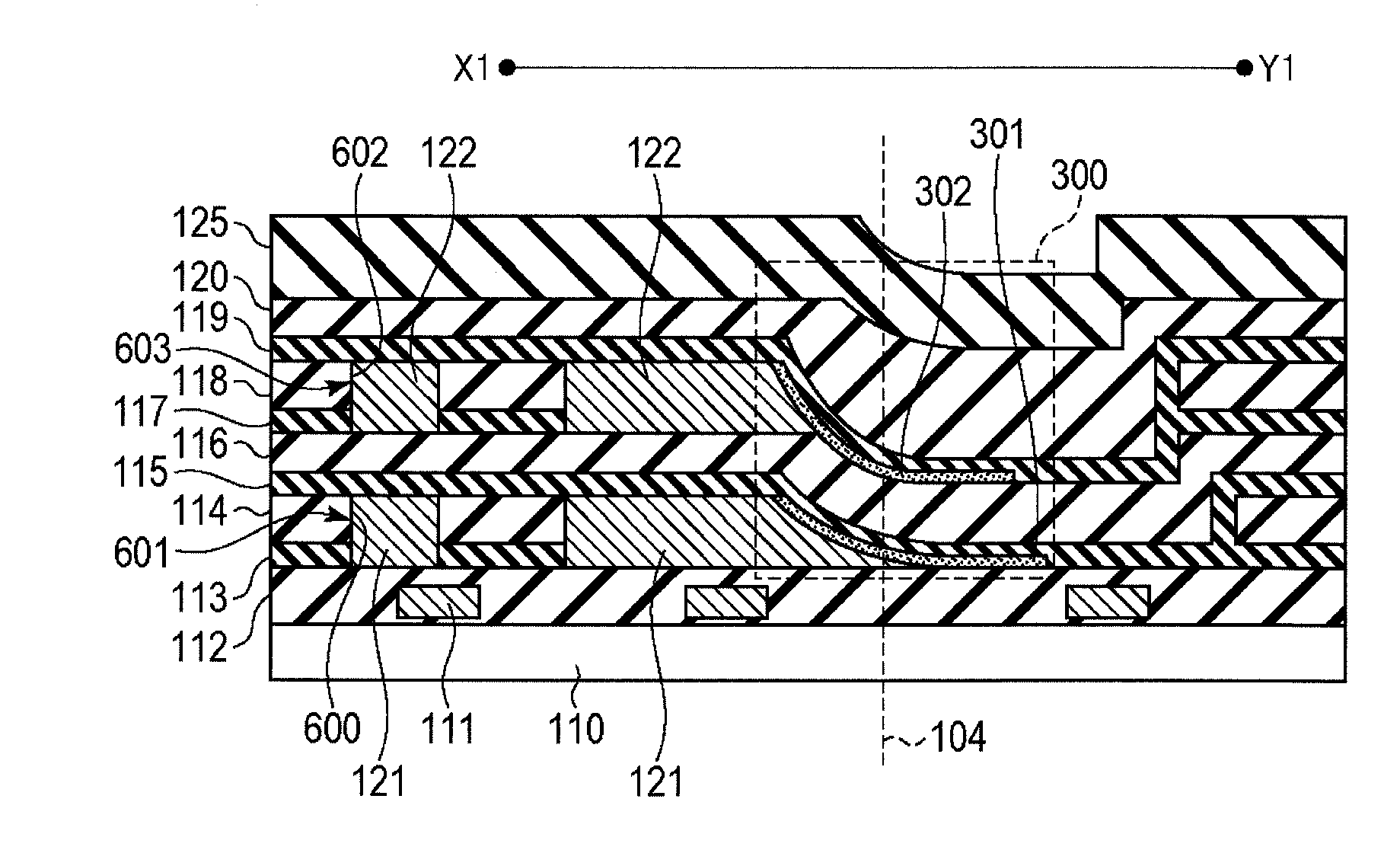
[0053]Hereinafter, a method of manufacturing a semiconductor device according to a first embodiment of the present invention will be described by using FIGS. 8A and 8B, FIGS. 9A to 9C, FIGS. 10A to 10C, FIGS. 11A and 11B, and FIG. 12. FIGS. 8A and 8B are schematic plan views for explaining mask patterns used in the method of manufacturing a semiconductor device according to the present embodiment. FIGS. 9A to 9C, FIGS. 10A to 10C, FIGS. 11A and 11B, and FIG. 12 are schematic cross sectional views illustrating the method of manufacturing a semiconductor device according to the present embodiment. Note that, constituent elements similar to those in the reference mode will be assigned with the same reference numerals, and the explanation thereof will be omitted or simplified. In addition, the drawings used for the explanation of the reference mode will be also referred to as needed.
[0054]The method of manufacturing a semiconductor device according to the present embodiment is character...
second embodiment
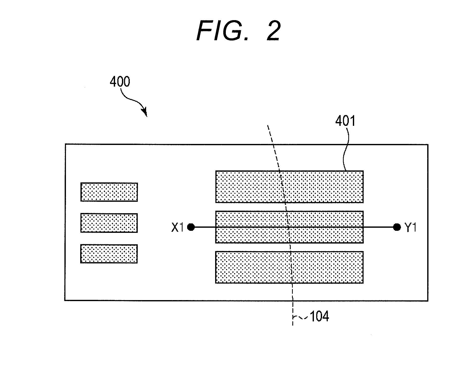
[0089]A semiconductor device according to a second embodiment of the present invention is described by using FIG. 13. FIG. 13 is a schematic plan view illustrating a configuration of the semiconductor device according to the present embodiment. Note that, constituent elements similar to those in the reference mode and the first embodiment will be assigned with the same reference numerals, and the explanation thereof will be omitted or simplified. In addition, the drawings used for the explanation of the reference mode will be referred to as needed.
[0090]In the present embodiment, a configuration of a solid-state image sensor will be described as an example of the semiconductor device of the present invention.
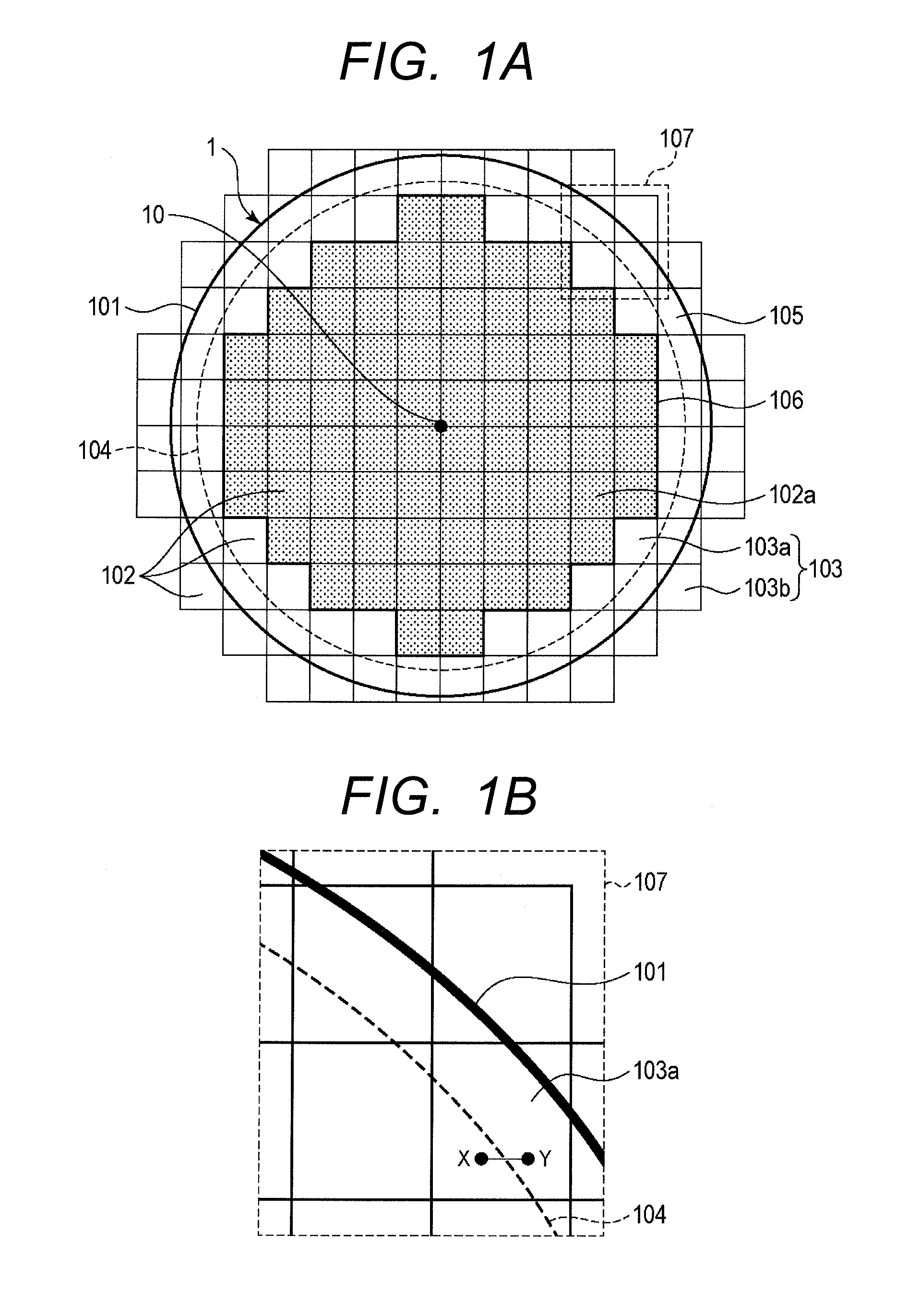
[0091]A solid-state image sensor 1000 according to the present embodiment corresponds to one segment (semiconductor device) 102 illustrated in FIG. 1A, and is a solid-state image sensor of a complementary metal oxide semiconductor (CMOS) type, for example. As illustrated in FIG....
modified embodiment
[0096]The present invention is not limited to the foregoing embodiments, but can be modified variously.
[0097]For example, the foregoing embodiments are described by taking, as an example, the case where the copper film is used as the conductive film filled into the recessed portions, but the conductive film is not limited to the copper film. The conductive film filled into the recessed portions may be any of films made of various metal materials that can form a wiring layer, besides a copper film or a copper alloy film containing copper as a main ingredient.
[0098]In addition, the foregoing embodiments are described by taking, as an example, the case where a single damascene process is employed as the damascene process for forming the wiring layer. Instead of this, the wiring layer and conductor plugs may be formed together and integrally by a dual damascene process, for example.
[0099]Moreover, the foregoing second embodiment is described by taking the solid-state image sensor as an ...
PUM
 Abstract
Description
Claims
Application Information