Device including a metallization layer and method of manufacturing a device

Active Publication Date: 2016-08-04
INFINEON TECH AG
View PDF2 Cites 15 Cited by
  • Summary
  • Abstract
  • Description
  • Claims
  • Application Information

AI Technical Summary

Benefits of technology

[0004]According to an embodiment, a device includes a base element, and a metallization layer over the base element, the metallization layer having pores and having a varying degree of porosity. The degree of porosity is higher in a portion adjacent to the base element than in a portion remote from the base element.
[0005]According to a further embodiment, a device includes a base element and a porous metallization layer over the base element. The metallization layer includes a metal from the group of copper, silver, nickel and gold and further includes a conductive fi

Problems solved by technology

In particular, due to their large electrical and thermal conductivity, copper metallization layers may conduct heat and current at low losses.
Further, cracks may form in the metallization layer and additionally, when processin

Method used


Image

  • Device including a metallization layer and method of manufacturing a device
  • Device including a metallization layer and method of manufacturing a device
  • Device including a metallization layer and method of manufacturing a device

Examples


Example

Example 1

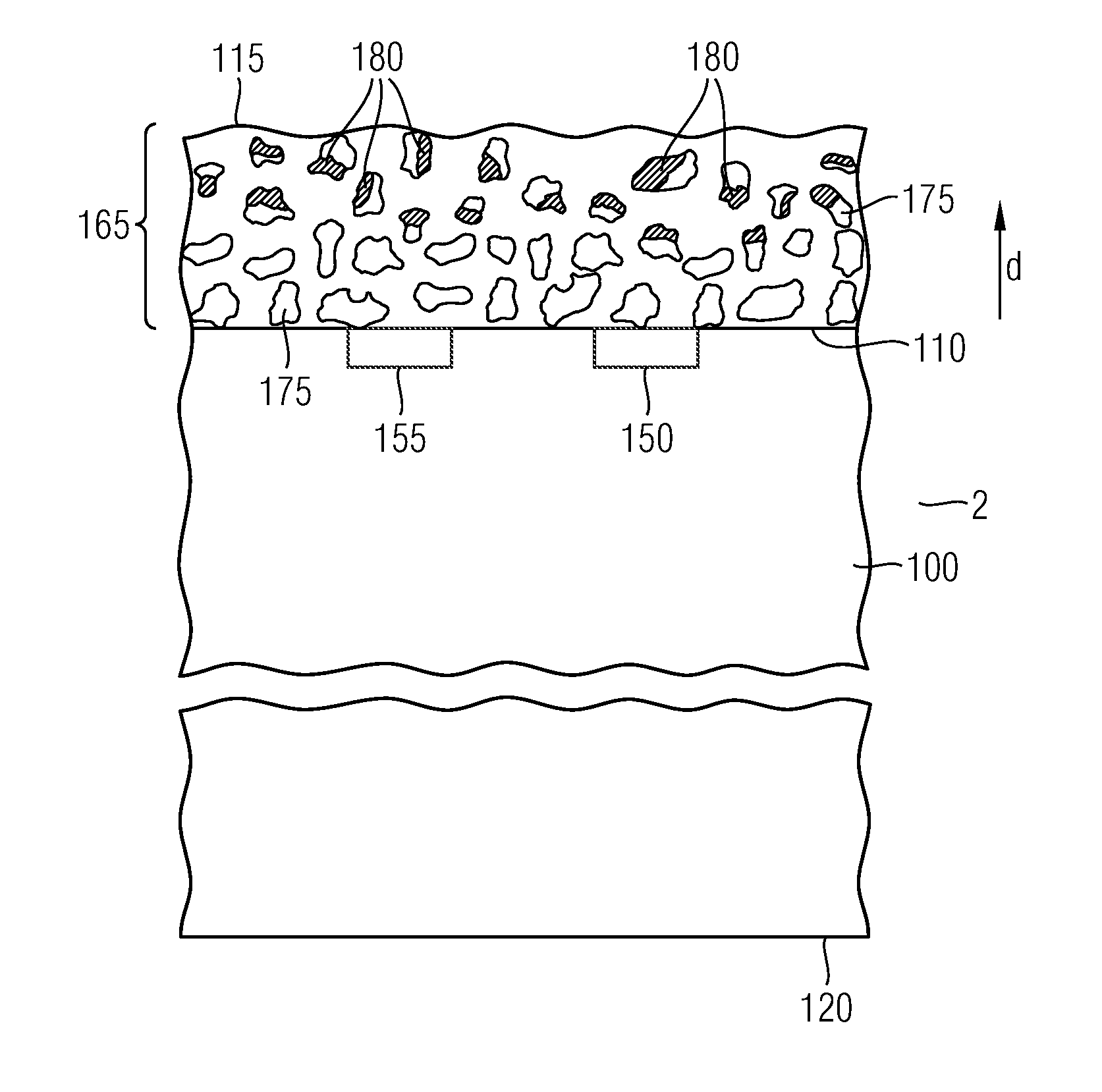
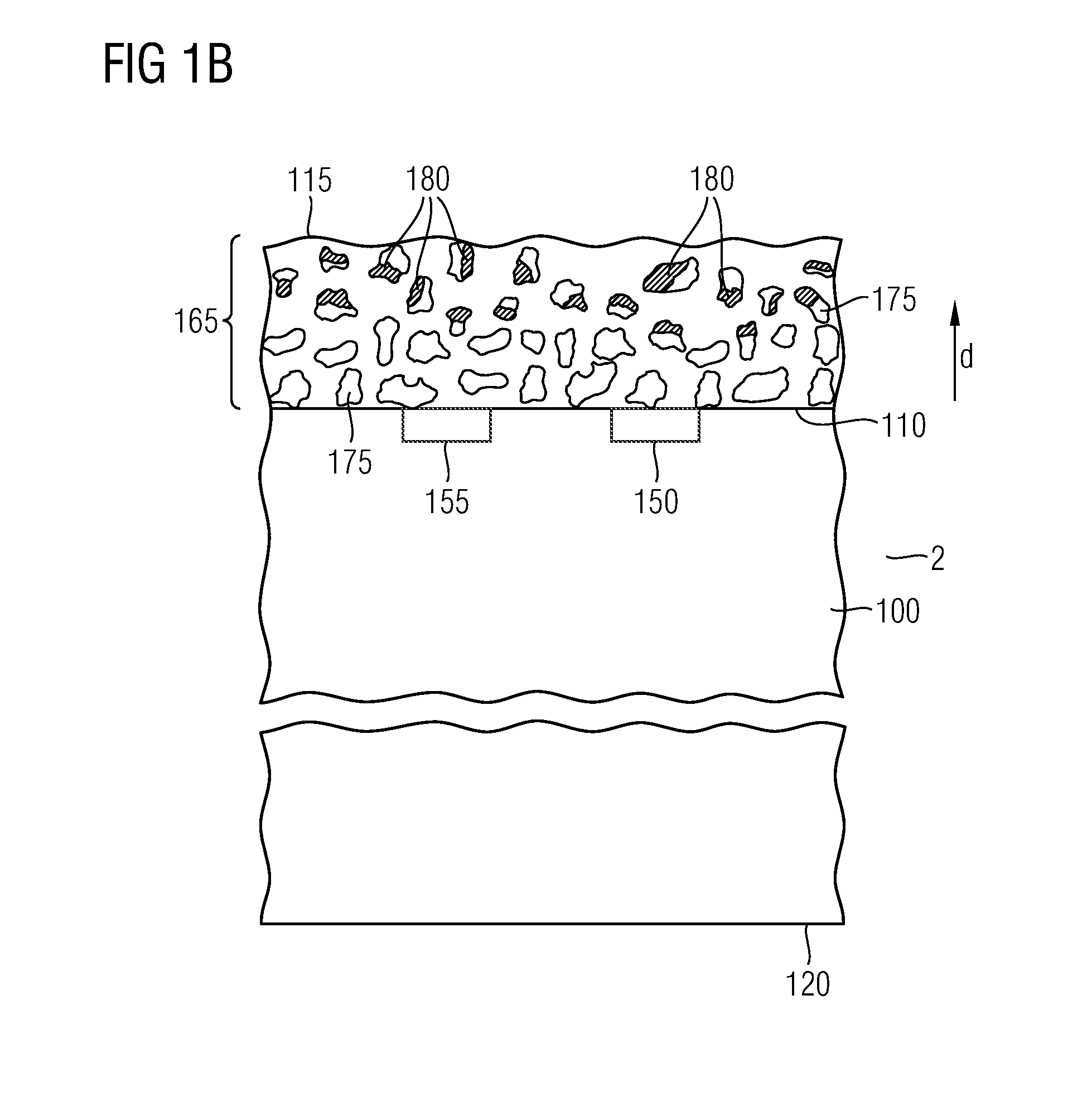
[0042]Starting material is a porous copper layer on an arbitrary carrier, e.g. a semiconductor wafer printed with a copper paste. The copper paste has been dried, sintered and annealed. This system defines a mechanical stable porous system. Thereafter, a copper nanoparticle ink may be applied, such as CI-002 (made by Intrinsiq Materials Inc.) using an inkjet printing process. For example, one layer of nanoparticles may be applied at a printing resolution of 495 dpi (“dots per inch”). The substrate temperature may be 35° C. and the following parameters may be set. Print head: 2 / 6 / 2 waveform (piezo); 87.2 V; 90%; −20 mbar; 30° C. head temperature; 35° C. substrate temperature. Thereafter, the metallization layer is dried at 100° C. for 15 minutes. Then, a sintering process is performed at 400° C., using 30 min. pre-heating time and 15 min. heating time at 400° C. at a N2 / CH2O2-atmosphere.

[0043]It has been shown that the applied nanoparticles are fused together or coalesced wi...

Example

Example 2

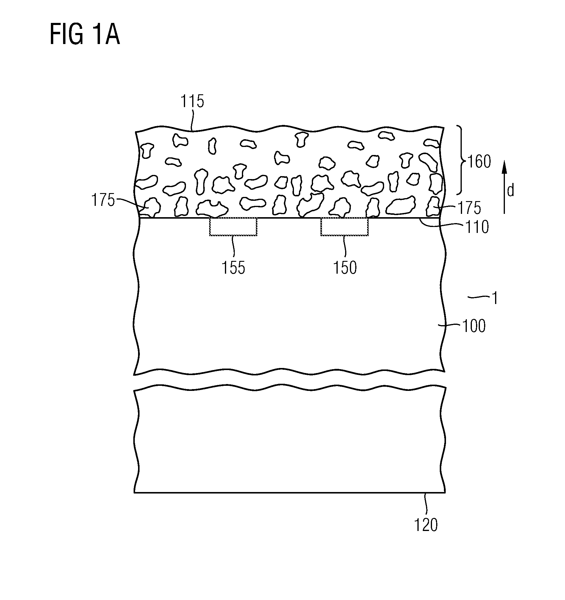
[0056]Starting material is an arbitrary carrier. For example, the carrier may be a semiconductor wafer comprising several device components 555, and, optionally, circuit elements 550 (cf. FIG. 5) as has been discussed above with reference to FIG. 1. For example, a barrier layer may be formed over the first surface 510 of the carrier 500. For example, if the semiconductor material is silicon, an unwanted chemical reaction between the silicon and the copper layer may be avoided due to the barrier layer. Thereafter, a first copper paste is applied to the carrier 500. For example, this may be accomplished by performing a stencil or a screen printing method, followed by a drying step (e.g. at 60° C. for 1 hour, depending on the paste properties) and further steps of sintering and annealing. As a result, a mechanical stabile porous system having a porosity of approximately 40 to 50% and a layer thickness of 10 to 50 μm may be obtained, depending on paste and stencil thickness. As...

Example

Example 3

[0070]Starting point for performing the method according to this embodiment is a base element similar to the base element described with reference to Example 2. First, a metal paste (e.g. CP-003 by Intrinsiq Materials Inc.) for forming a metal layer having a high degree of porosity is applied. This may be accomplished using a paste printing method (stencil or screen print). Then, a drying process and an annealing step may be performed so as to form a mechanical stabile porous system having a porosity of approximately 40-50%. The process parameters may be as described with reference to Example 1. The metal layer may have a thickness of approximately 10 to 50 μm. Thereafter, a metal organic copper precursor compound may be applied.

[0071]According to an example, a copper oximate may be used. A heat treatment to a temperature sufficient to decompose the copper oximate may be performed. For example, the base element may be heated to a temperature of approximately 180° C. As a re...


PUM


Abstract

A device comprises a base element and a metallization layer over the base element. The metallization layer comprises pores and has a varying degree of porosity, the degree of porosity being higher in a portion adjacent to the base element than in a portion remote from the base element.

Description

TECHNICAL BACKGROUND[0001]In the field of metallization layers, e.g., for use in semiconductor devices, for example, power semiconductor devices, metallization layers having a large thickness are employed for conducting large currents and for transferring heat. In particular, due to their large electrical and thermal conductivity, copper metallization layers may conduct heat and current at low losses. The electrical and thermal conductivity is increased by increasing the thickness of a metallization layer. However, due to the different thermal expansion coefficients of a metallization layer with respect to the material of a carrier on which the metallization layer is disposed, delamination of the metallization layer may occur. Further, cracks may form in the metallization layer and additionally, when processing a semiconductor wafer on which a thick metallization layer is arranged, the wafer may bow so that a further processing becomes difficult.[0002]Metallization layers which are ...

Claims


Application Information

Patent Timeline
IPC IPC(8): H01L23/532H01L21/768
CPCH01L21/76883H01L23/53228H01L23/522H01L23/53209H01L24/83H01L21/288H05K1/09H05K1/11H05K3/22
Inventor MISCHITZ, MARTINHEINRICI, MARKUSSCHWAB, STEFAN
Owner INFINEON TECH AG
Why Eureka
Try Eureka