Semiconductor device comprising an ESD protection circuit

a protection circuit and electrostatic discharge technology, applied in semiconductor devices, diodes, transistors, etc., can solve the problems of gate oxide damage, failure of the semiconductor device, and difficult to achieve cross-domain electrostatic discharge protection in advanced semiconductor technology nodes, etc., to enhance the normal operation of the device, enhance the device's robustness, and reduce the resistance

a protection circuit and electrostatic discharge technology, applied in semiconductor devices, diodes, transistors, etc., can solve the problems of gate oxide damage, failure of the semiconductor device, and difficult to achieve cross-domain electrostatic discharge protection in advanced semiconductor technology nodes, etc., to enhance the normal operation of the device, enhance the device's robustness, and reduce the resistance

US20160225758A1Active Publication Date: 2016-08-04NXP BV

Image

  • Semiconductor device comprising an ESD protection circuit
  • Semiconductor device comprising an ESD protection circuit
  • Semiconductor device comprising an ESD protection circuit

Examples


Embodiment Construction

[0040]Embodiments of the present invention are described in the following with reference to the accompanying drawings.

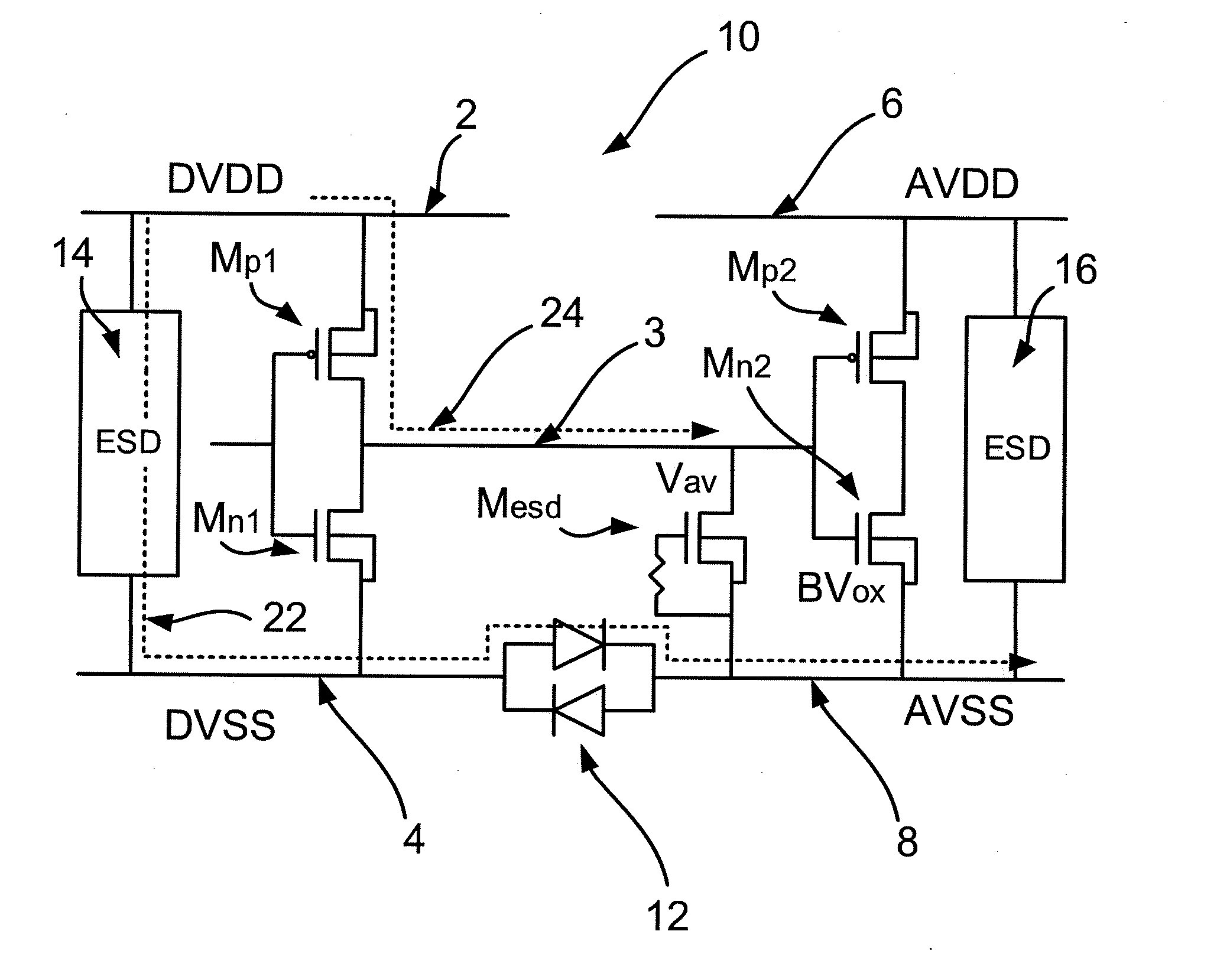
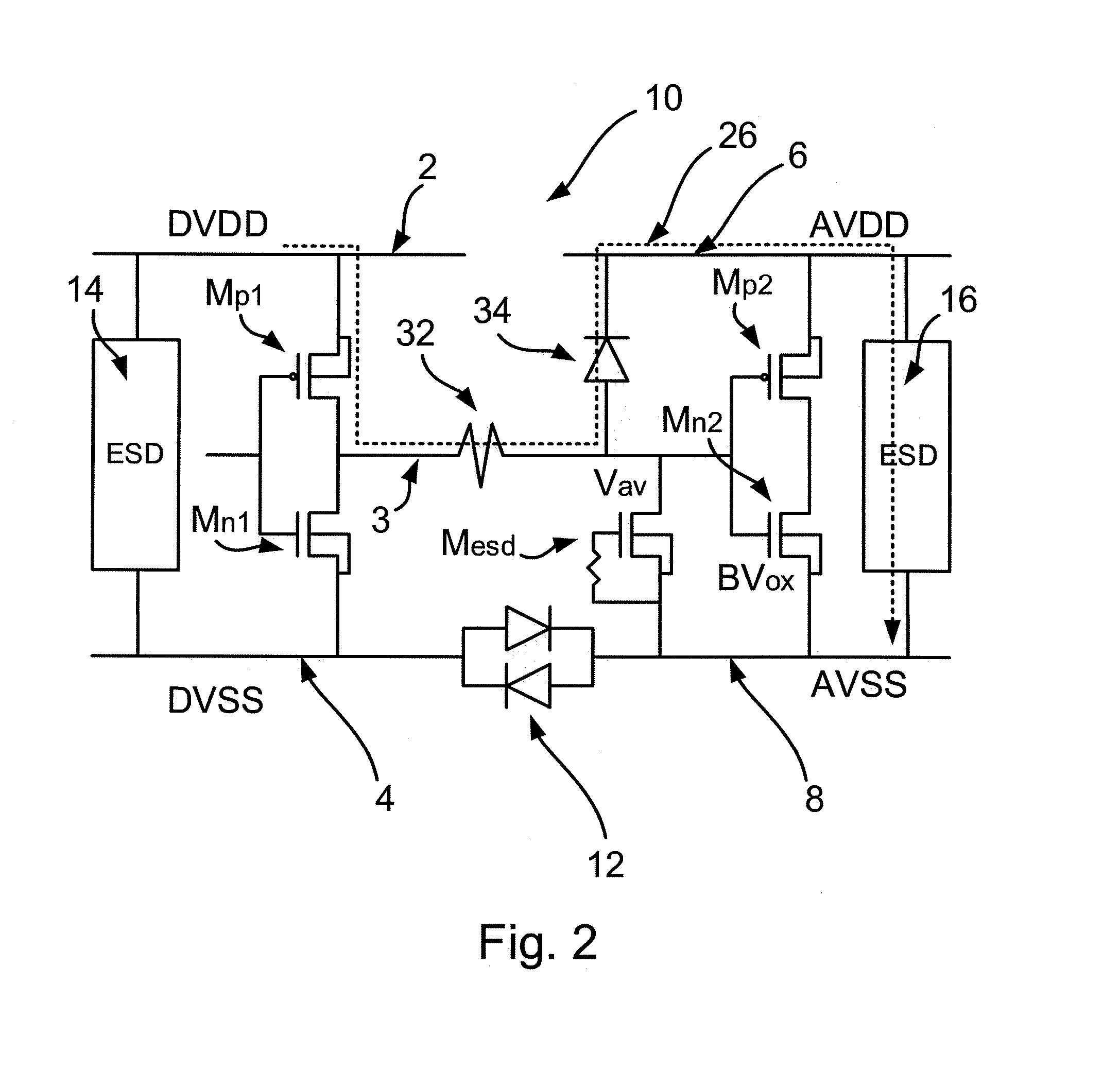
[0041]Embodiments of this invention can provide a semiconductor device including a first domain and a second domain that are provided with ESD protection by a protection circuit that includes a blocking transistor. The blocking transistor may be connected between the first domain power rail and a signal line of the semiconductor device for preventing current passing from the first domain power rail to the signal line in an ESD event. On the other hand, the blocking transistor may remain switched on during normal operation of the device. A power rail clamp may be connected between the first domain power rail and the first domain ground rail to allow an ESD current to discharge from the first domain power rail to the first domain ground rail during an ESD event. hi accordance with an embodiment of this invention, the power rail clamp is also operable to control the blo...


PUM


Abstract

A semiconductor device and method. The device includes a first domain and a second domain each having a power rail and a ground rail. The device further includes a signal line connected between the first domain and the second domain. The device also includes an electrostatic discharge protection circuit for providing cross-domain ESD protection. The protection circuit includes a blocking transistor connected between the first domain power rail and the signal line. The protection circuit also includes a power rail clamp connected between the first domain power rail and the first domain ground rail. The power rail clamp is operable to apply a control signal to a gate of the blocking transistor to switch it on during normal operation and to switch it off during an ESD event. The power rail clamp is operable during the ESD event to conduct an ESD current.

Description

FIELD OF THE INVENTION[0001]This invention relates to a semiconductor device comprising an electrostatic discharge (ESD) protection circuit.BACKGROUND OF THE INVENTION[0002]Cross domain electrostatic discharge (ESD) protection is becoming difficult to achieve in advanced semiconductor technology nodes due to a number of challenges, most commonly associated with the ever smaller size of devices such as transistors provided in an integrated circuit.[0003]FIG. 1 shows an example of a conventional semiconductor device 10. The device has a digital domain that includes a digital domain power rail 2 and a digital domain ground rail 4 (these are also labelled DVDD and DVSS in FIG. 1, respectively). The device 10 also includes an analogue domain that has an analogue domain power rail 6 and an analogue domain ground rail 8 (these are also labelled AVDD and AVSS in FIG. 1, respectively). The digital domain and the analogue domain may form part of a mixed signal device.[0004]The digital domain ...

Claims


Application Information

Patent Timeline
04 Aug 2016
Publication
US20160225758A1
IPC
H01L27/02; H02H9/04; H01L27/092
CPC
H01L27/0251; H01L27/0292; H02H9/046; H01L27/092; H01L27/0255; H01L27/0266
Inventors
LAI, DA-WEI; ABESSOLO BIDZO, DOLPHIN