
Eureka
For R&D, Eureka makes reading and utilizing patents & technical documents easy.
Eureka AIR
Designed for self-driven R&D workflows. Generate viable solutions, solve complex R&D challenges, empower your innovation with AI.

Eureka Materials
Designed for material experts only. Revolutionize your material R&D, from search, analyze, to developing new materials.

TechResearch
Generate reliable direction feasibility study reports for your R&D in just a few steps.

TechSeek
Discover and master advanced knowledge NOW. Basics, ideas, possibilities, all at once.

TechMind
As an expert in R&D Theories, TechMind can generates customized viable solutions instantly.

TechRisk
Analyze your overall solution with one click, know your potential R&D risks in advance.

TechMonitor
Get weekly tech updates, stay abreast of the latest tech innovations and key insights.
Method for manufacturing semiconductor device
a manufacturing method and semiconductor technology, applied in the direction of semiconductor devices, electrical appliances, transistors, etc., can solve problems such as transistor electric characteristics defects, and achieve the effect of improving the reliability of the semiconductor device using the oxide semiconductor and improving the electric characteristics of the semiconductor devi
- Summary
- Abstract
- Description
- Claims
- Application Information
AI Technical Summary
Benefits of technology
Problems solved by technology
Method used
Image

Examples
embodiment 1
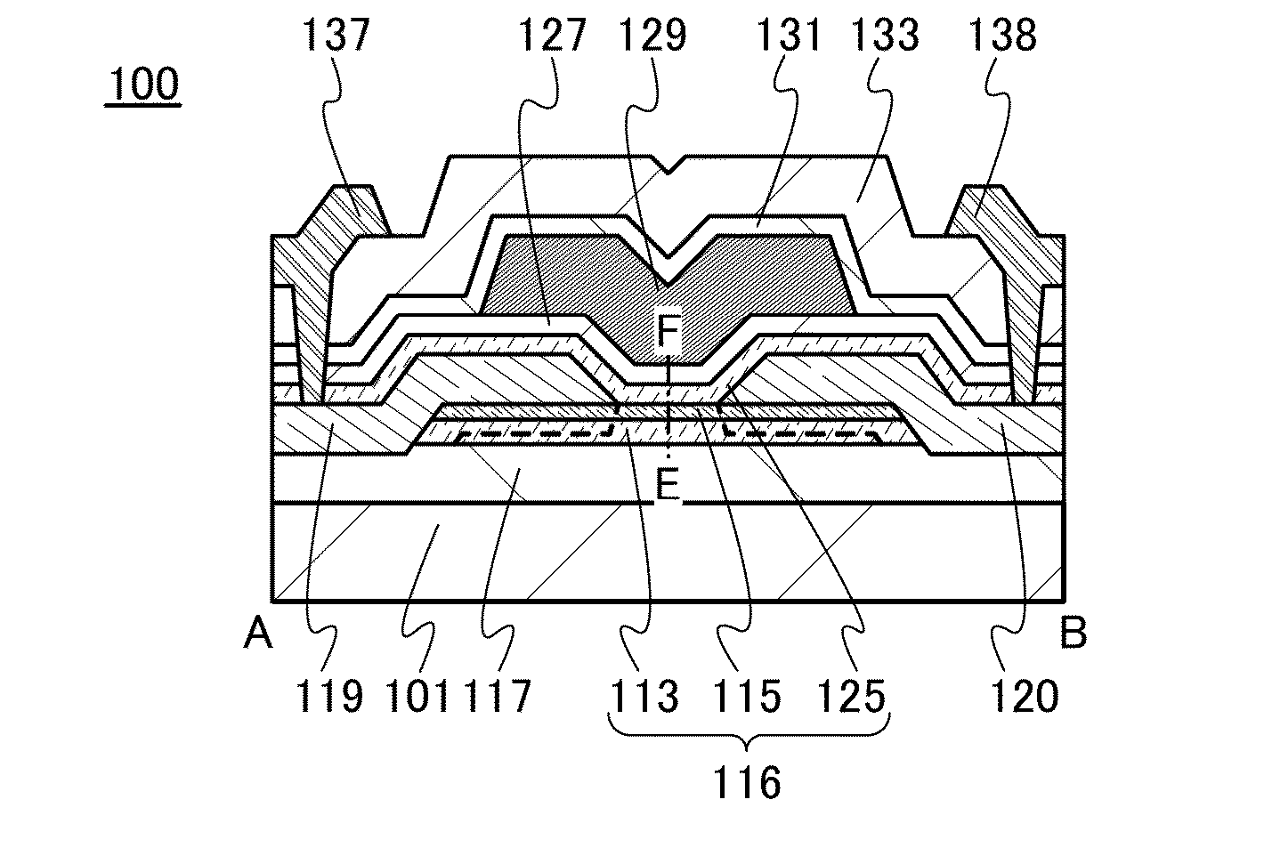
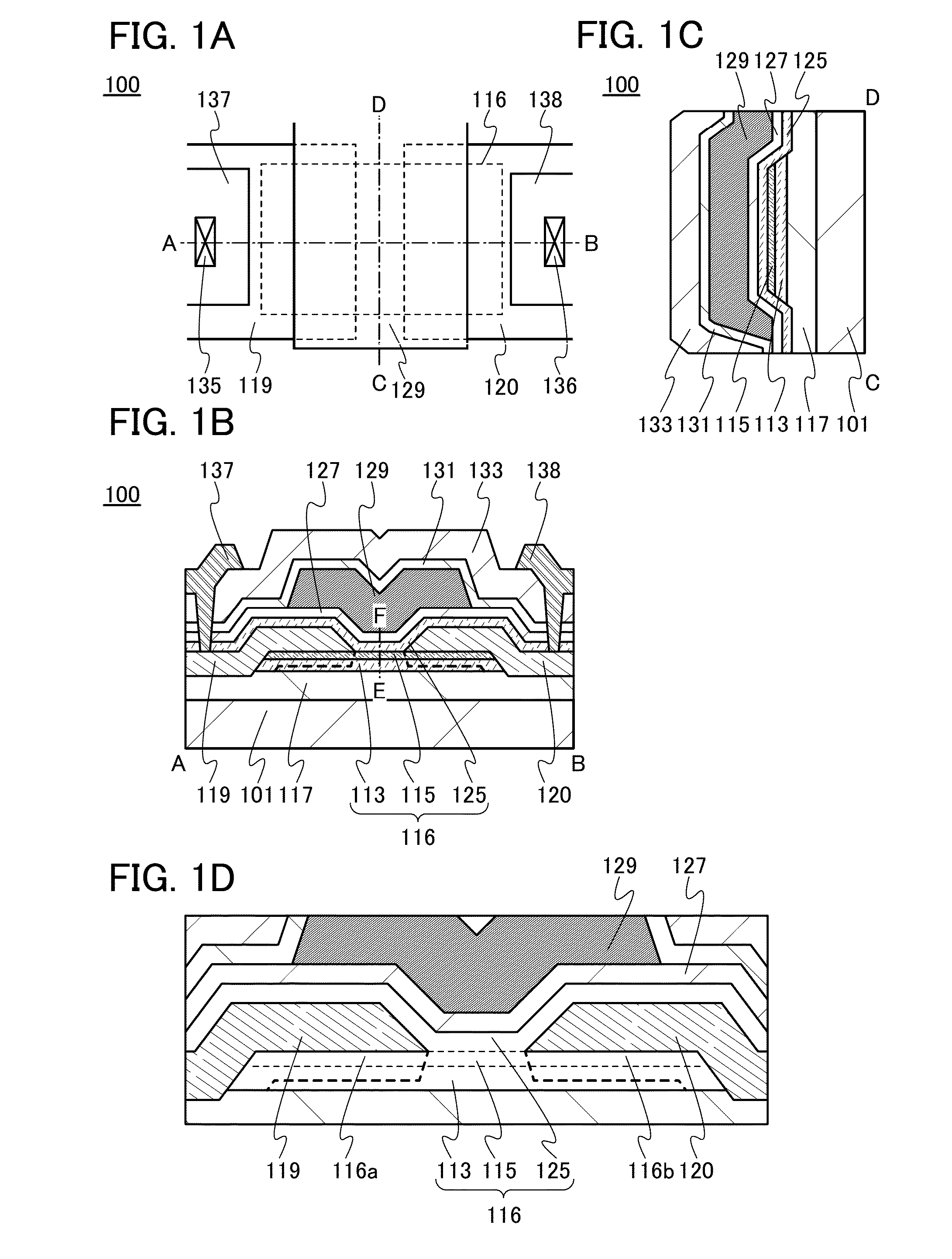
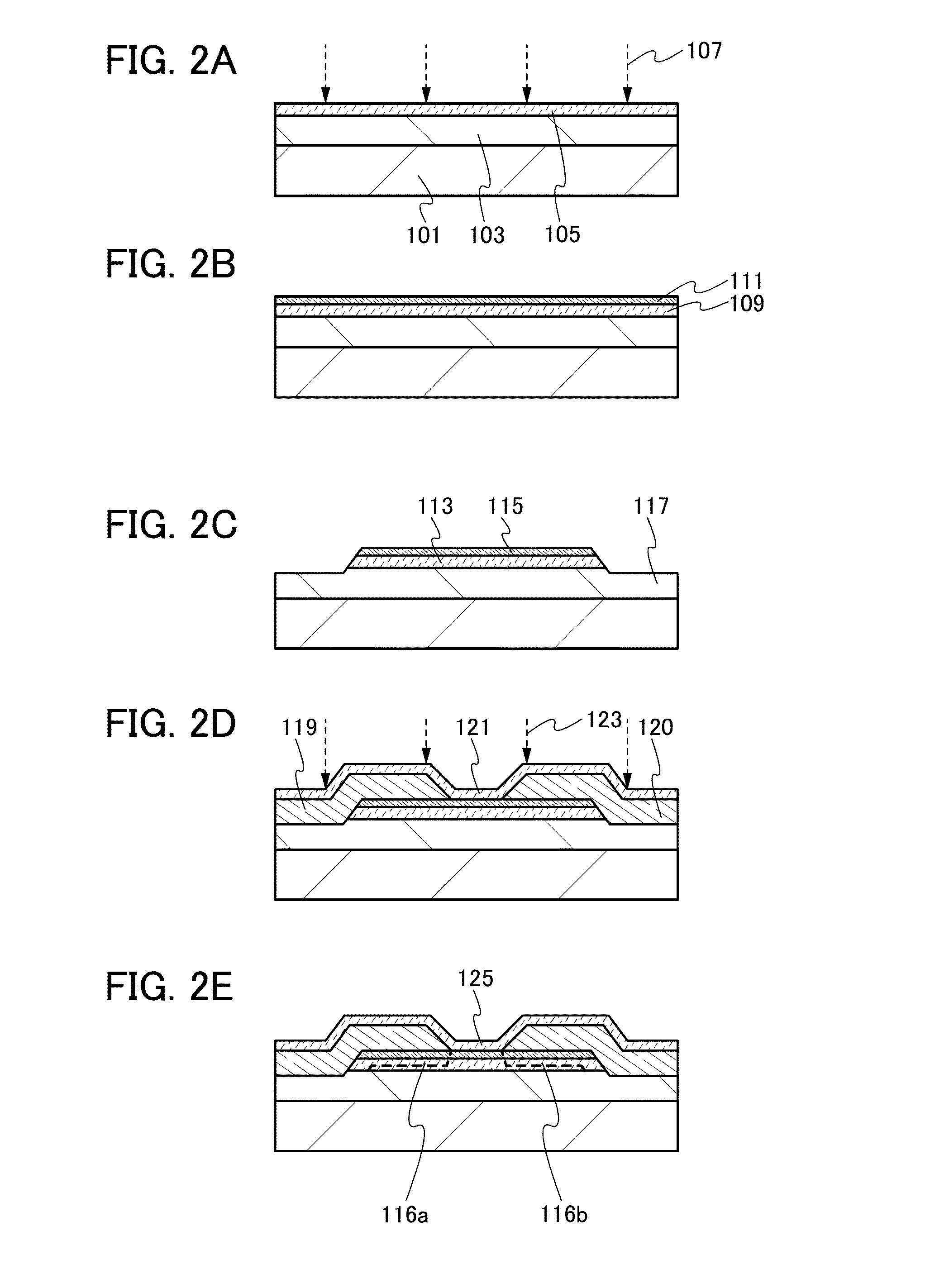
[0064]The threshold voltage of a transistor using an oxide semiconductor film with oxygen vacancies easily shifts negatively, and such a transistor tends to be normally-on. This is because electric charges are generated owing to oxygen vacancies in the oxide semiconductor, and the resistance is reduced. In addition, a transistor using an oxide semiconductor film with oxygen vacancies has such a problem that the electric characteristics, typically, the threshold voltage, are changed with time or changed by a stress test (typically, a gate bias-temperature (BT) stress test under light irradiation). In this embodiment, a highly reliable semiconductor device in which a change in threshold voltage is small and a manufacturing method thereof will be described. Further, a semiconductor device with excellent electric characteristics and a manufacturing method thereof will be described.
[0065]In this embodiment, a method for manufacturing a top-gate transistor is described.
[0066]FIGS. 1A to 1...
modification example 6
[0224]In the transistor in this embodiment, the pair of electrodes 119 and 120 is provided between the oxide semiconductor film 115 and the oxide film 125; however, the pair of electrodes 119 and 120 may be provided between the oxide insulating film 117 and the oxide film 113.
modification example 7
[0225]An insulating film that can be used as the oxide insulating film 117 functioning as a base insulating film in this embodiment is described below.
[0226]The oxide insulating film 117 can be formed using an oxide insulating film whose oxygen content is in excess of that in the stoichiometric composition. In other words, an oxide insulating film from which part of contained oxygen is released by heating can be formed. With use of such a film, the oxygen in the oxide insulating film 117 is transferred to the oxide semiconductor film 115; thus, the density of defect levels at the interface between the oxide insulating film 117 and the oxide film 113 can be reduced, and oxygen vacancies can be further reduced by filling oxygen vacancies in the oxide semiconductor film 115. For example, when an oxide insulating film having the following feature is used, the density of defect levels at the interface between the oxide insulating film 117 and the oxide film 113 can be decreased and oxyge...
PUM
 Abstract
Description
Claims
Application Information
 - R&D Engineer
- R&D Manager
- IP Professional
- Industry Leading Data Capabilities
- Powerful AI technology
- Patent DNA Extraction
Browse by: Latest US Patents, China's latest patents, Technical Efficacy Thesaurus, Application Domain, Technology Topic, Popular Technical Reports.
© 2024 PatSnap. All rights reserved.Legal|Privacy policy|Modern Slavery Act Transparency Statement|Sitemap|About US| Contact US: help@patsnap.com