Semiconductor device and operating method thereof

a technology of semiconductor devices and operating methods, applied in the direction of digital storage, memory adressing/allocation/relocation, instruments, etc., can solve the problems of excessively large mapping tables, reducing the efficiency of using the entire storage space, etc., to reduce the number of erase operations, write operations, garbage collection, and reduce the size of mapping tables.

Active Publication Date: 2016-09-08
SK HYNIX INC +1
View PDF2 Cites 7 Cited by
  • Summary
  • Abstract
  • Description
  • Claims
  • Application Information

AI Technical Summary

Benefits of technology

[0031]The address mapping device and the operation method thereof according to the present technology are employed, so as to reduce the size of a mapping table. When a request is concentrated on a specific logical address region, a physical address region corresponding to the logical address region is dynamically expanded, so as to reduce the number of erase operations, write operations, and garbage collections.
[0032]Consequently, when a storage space is limited as with a mobile device it is possible to reduce the waste of the storage space due to an increase in the size of a mapping table and to substantially prevent performance degradation due to frequent background operations.

Problems solved by technology

As described above, the page mapping technology has a problem where as the number of physical pages (i.e., the size of the memory cell array 4) increases, the size of the mapping table 30 excessively increases.
However, also in the partition recognition mapping technology, when a request is concentrated on a specific partition, the corresponding partition is quickly consumed as compared with other partitions, thereby reducing efficiency in using the entire storage space.

Method used


Image

  • Semiconductor device and operating method thereof
  • Semiconductor device and operating method thereof
  • Semiconductor device and operating method thereof

Examples


Embodiment Construction

[0042]Hereinafter, a semiconductor device and an operation method thereof according to the present invention will be described in detail with reference to the accompanying drawings through exemplary embodiments.

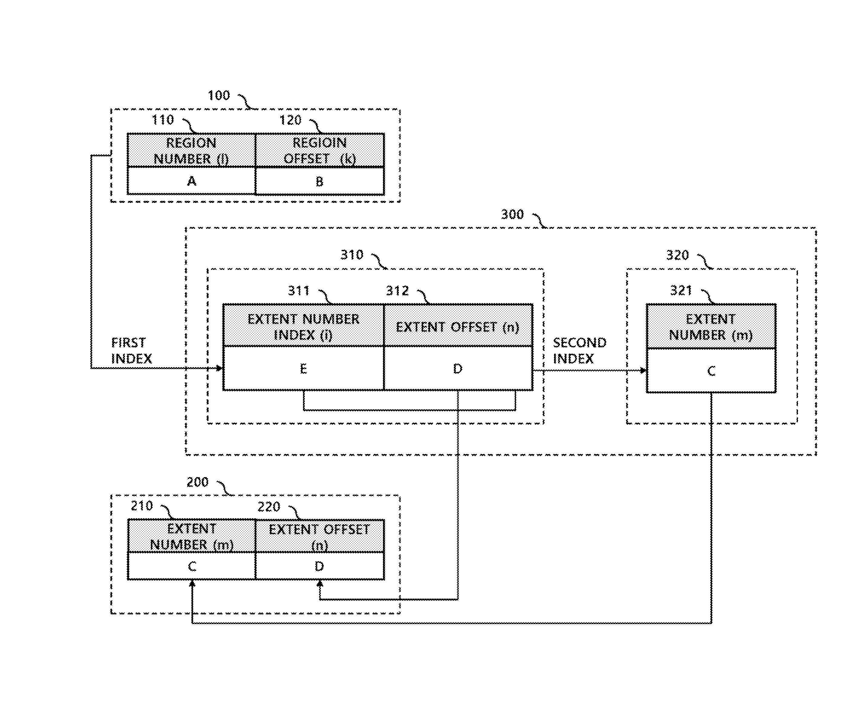
[0043]FIG. 5 is a diagram explaining a mapping technology according to an embodiment of the present invention.

[0044]In the present invention, a logical address 100 managed by a host 1 is hierarchized into a region number 110 and a region offset 120, and a physical address 200 managed by a memory device 2 is hierarchized into an extent number 210 and an extent offset 220. Hereinafter, an address indicates a page address.

[0045]In the present invention, a mapping table 300 includes a first table 310 and a second table 320.

[0046]The second table 320 stores a corresponding relation between the region number 110 and an extent number 321. In the present embodiment, an index (a second index) of the second table 320 is divided in units of the maximum number of extents allocable to a r...


PUM


Abstract

A semiconductor device includes a mapping table that stores a corresponding relation between a logical address defined on a basis of regions and a physical address defined on a basis of extents, wherein one or more extents are dynamically allocated to one region.

Description

[0001]The present application claims priority under 35 U.S.C. §119(a) to Korean application number 10-2015-0028785, filed on Mar. 2, 2015, in the Korean Intellectual Property Office, which is incorporated herein by reference in its entirety as set forth in full.BACKGROUND[0002]1. Technical Field[0003]The present invention relates to a semiconductor device and an operation method thereof. Particularly, the present invention relates to a semiconductor device that controls mapping between a logical address requested from a host and a physical address of a memory device, and an operation method thereof.[0004]2. Related Art[0005]FIG. 1 is a block diagram illustrating a general memory system. The memory system may include a host 1 and a memory device.[0006]The host 1 designates a logical address and requests the memory device 2 to perform a read / write operation. The memory device may include a control unit 3, a memory cell array 4, and a mapping table, The control unit 3 finds a physical ...

Claims


Application Information

Patent Timeline
Patent Type & Authority Applications(United States)
IPC IPC(8): G06F12/02
CPCG06F12/0292G06F2212/7201G06F2212/1041G11C8/06G11C16/10G11C16/26G06F12/0246G06F12/06G06F12/1009
Inventor LEE, TAE-HWAJOE, YOON-JANGCHA, JAE-HYUK
Owner SK HYNIX INC
Why Eureka
Try Eureka