Supercharge Your Innovation With Domain-Expert AI Agents!

Organic light emitting display device

a light-emitting display device and organic technology, applied in the field of display technology, can solve the problems of inability to completely remove moisture and escape moisture, and achieve the effect of prolonging the service life and improving the ageing and shrinkage of some pixels in the organic light-emitting display devi

Active Publication Date: 2016-09-08
BOE TECH GRP CO LTD
View PDF8 Cites 11 Cited by
  • Summary
  • Abstract
  • Description
  • Claims
  • Application Information

AI Technical Summary

Benefits of technology

The present invention provides an organic light emitting display device with a longer service life. By including a first pixel defining layer doped with a desiccant in the device, heat generated during the lighting process helps to absorb moisture that may escape from the thin film transistor array substrate or other functional layers. This improves the ageing and shrinkage of pixels and prolongs the lifespan of the organic light emitting display device.

Problems solved by technology

However, in the prior art, although part of moisture in the thin film transistor array substrate 1 and the color filter layer 3 is removed by roasting during fabrication, it is unable to remove the moisture completely.
Therefore, there is moisture escape during the use of the organic light emitting display device.

Method used


Image

  • Organic light emitting display device
  • Organic light emitting display device

Examples


embodiment 1

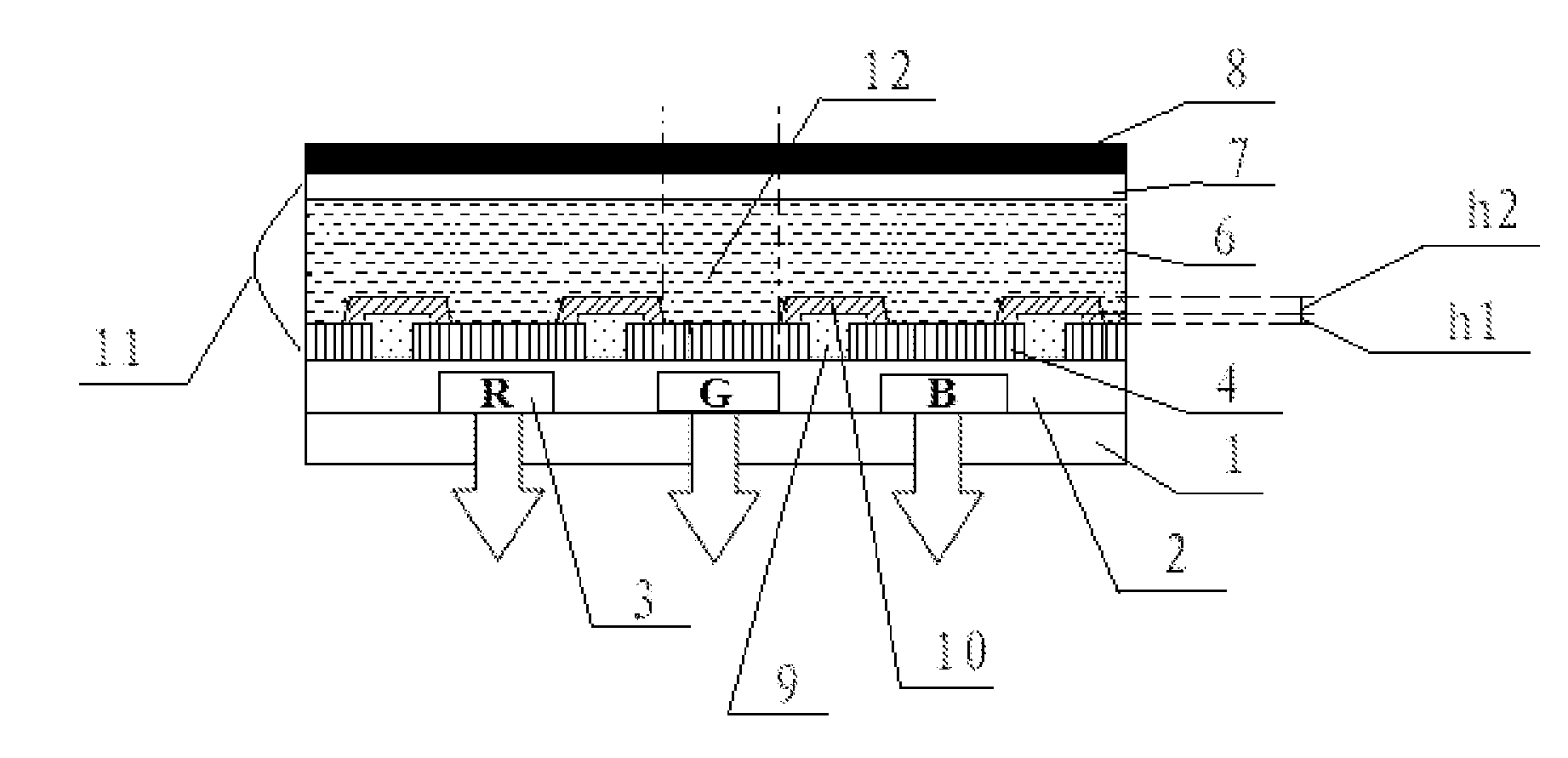
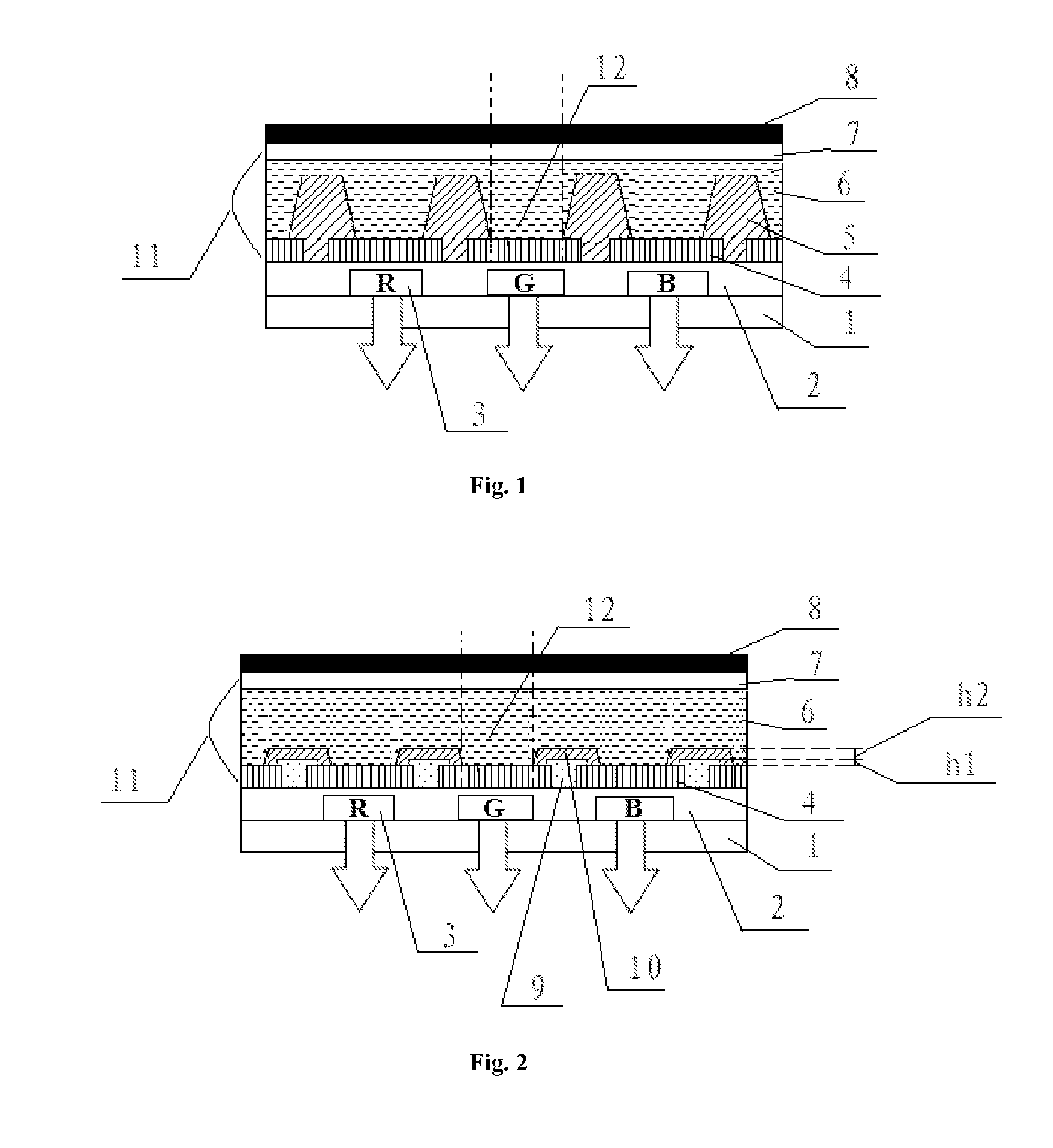
[0058]This embodiment provides an organic light emitting display device as shown in FIG. 2, including a thin film transistor array substrate 1, a planarization layer 2, a color filter layer 3, an anode 4, pixel defining layers, an organic light emitting layer 6, a cathode 7 and an encapsulating layer 8. The pixel defining layers include a second pixel defining layer 10 close to the organic light emitting layer 6 and a first pixel defining layer 9 away from the organic light emitting layer 6; and the first pixel defining layer 9 is doped with a desiccant.

[0059]The anode 4 is an Indium Tin Oxide (ITO) electrode, and the organic light emitting layer 6 is in a type of full-fluorescence light emission. Except the pixel defining layers, the fabrication of the above film layers is within the scope the prior art and will not be described herein.

[0060]The fabrication of the pixel defining layers will be introduced as below. The pixel defining layers include a first pixel defining layer 9 and...

embodiment 2

[0061]This embodiment provides an organic light emitting display device as shown in FIG. 2, including a thin film transistor array substrate 1, a planarization layer 2, a color filter layer 3, an anode 4, pixel defining layers, an organic light emitting layer 6, a cathode 7 and an encapsulating layer 8. The pixel defining layers include a second pixel defining layer 10 close to the organic light emitting layer 6 and a first pixel defining layer 9 away from the organic light emitting layer 6; and the first pixel defining layer 9 is doped with a desiccant.

[0062]The anode 4 is an Indium Tin Oxide (ITO) electrode, and the organic light emitting layer 6 is in a type of full-phosphorescence light emission. Except the pixel defining layers, the fabrication of the above film layers is within the scope of the prior art and will not be described herein.

[0063]The fabrication method of the pixel defining layers will be introduced as below. The pixel defining layers include a first pixel definin...

embodiment 3

[0064]This embodiment provides an organic light emitting display device as shown in FIG. 2, including a thin film transistor array substrate 1, a planarization layer 2, a color filter layer 3, an anode 4, pixel defining layers, an organic light emitting layer 6, a cathode 7 and an encapsulating layer 8. The pixel defining layers include a second pixel defining layer 10 close to the organic light emitting layer 6 and a first pixel defining layer 9 away from the organic light emitting layer 6; and the first pixel defining layer 9 is doped with a desiccant.

[0065]The anode 4 is an Indium Tin Oxide (ITO) electrode, and the organic light emitting layer 6 is in a type of combination of phosphorescence and fluorescence light emission. Except the pixel defining layers, the fabrication of the above film layers is within the scope of the prior art and will not be described herein.

[0066]The fabrication method of the pixel defining layers will be introduced as below. The pixel defining layers in...


PUM


Abstract

The present invention provides an organic light emitting display device, belonging to the field of display technology, being capable of solving the problem, in an existing organic light emitting display device, of shortened service life of an organic light emitting diode due to moisture escape from the thin film transistor layer or the like. The organic light emitting display device of the present invention comprises a first pixel defining layer doped with a desiccant, which absorbs moisture escaping from an array substrate or the like during the use of the organic light emitting display device, thus improving the ageing and shrinkage of some pixels in the organic light emitting display device and prolonging the service life of the organic light emitting display device.

Description

FIELD OF THE INVENTION[0001]The present invention belongs to the field of display technology, and particularly to an organic light emitting display device.BACKGROUND OF THE INVENTION[0002]An organic Light Emitting Diode (OLED), as an organic thin film electroluminescent device, has the advantages of simple fabrication process, low cost, high luminous efficiency, ease of formation of a flexible structure, and the like. Hence, the display technology of the organic light emitting diode becomes a hot spot to be researched and developed.[0003]An organic light emitting diode display device includes a plurality of pixel units, each of the pixel units consists of a plurality of sub-pixel units being adjacent to each other and emitting light of different colors, and each of the sub-pixel units being provided with one organic light emitting diode therein. The light emitting intensity of organic light emitting diodes may be controlled by controlling the current of each of the organic light emi...

Claims


Application Information

Patent Timeline
Patent Type & Authority Applications(United States)
IPC IPC(8): H01L27/32
CPCH01L27/326H01L27/3246H10K59/122H10K59/874H10K50/846H10K59/121
Inventor JIAO, ZHIQIANG
Owner BOE TECH GRP CO LTD
Features
  • R&D
  • Intellectual Property
  • Life Sciences
  • Materials
  • Tech Scout
  • Unparalleled Data Quality
  • Higher Quality Content
  • 60% Fewer Hallucinations
Learn More