Shift register unit and gate driving circuit

a technology of shift register and gate driving circuit, which is applied in the field of communication, can solve the problems of large volume of liquid crystal display, and achieve the effects of saving wiring space, suppressing output errors, and enhancing the output characteristic of shift register and service life of transistors

Active Publication Date: 2016-09-15
BOE TECH GRP CO LTD +1
View PDF1 Cites 39 Cited by
  • Summary
  • Abstract
  • Description
  • Claims
  • Application Information

AI Technical Summary

Benefits of technology

[0013]There provide a shift register unit and a gate driving circuit according to the embodiments of the present disclosure, the shift register unit comprises the input module, the reset module, the output module, the pull-down control module and the pull-down module, wherein the input module is connected to the input signal terminal and is configured to provide the first voltage signal to the output terminal in response to the input signal; the reset module is connected to the reset signal terminal and is configured to provide the second voltage signal to the input module as the first node of the output terminal of the input module in response to the reset signal; the output module is configured to provide the first clock signal to the output terminal in response to the voltage at the first node; the pull-down control module is configured to provide the second clock signal to the second node of the pull-down control module in response to the second clock signal, provide the power supply negative voltage to the second node in response to the voltage at the first node, and provide the power supply negative voltage to the second node in response to the voltage at the output terminal; and the pull-down module is configured to provide the power supply negative voltage to the first node and the output terminal in response to the voltage at the second node. By using a small number of thin film transistors, the shift register unit, realizes a signal transmitting function and a noise reducing function of the shift register unit, suppresses an output error due to drift of threshold voltages of elements per se and interferences of adjacent elements, and further enhances the output characteristic of the shift register and service life of the transistors; at the same time, the wiring space is saved because of the use of a small number of thin film transistors, which is beneficial to reduce the size of the shift register unit, so as to reduce the volume of the whole liquid crystal display.

Problems solved by technology

However, change of respective alternating current clock signals in the gate driving circuit will cause interference noise to occur in the circuit, which affects the output of signal and the stability of the shift register unit; at the same time, a greater number of thin film transistors need a larger wiring space, so that the whole shift register unit has a big size, thereby causing that the liquid crystal display has a large volume.

Method used


Image

  • Shift register unit and gate driving circuit
  • Shift register unit and gate driving circuit
  • Shift register unit and gate driving circuit

Examples


first embodiment

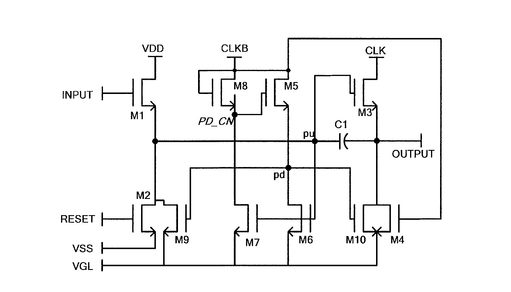
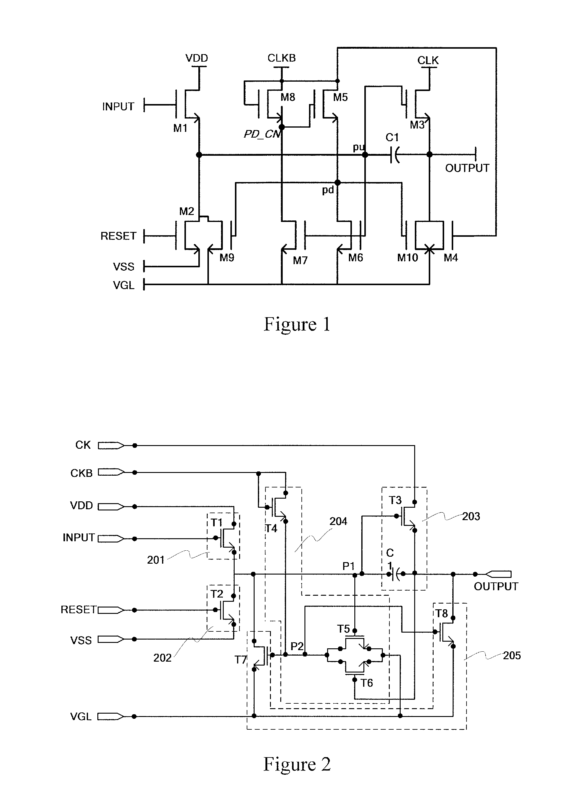
[0022]According to the present disclosure, there is provided a shift register unit, and its structure is as shown in FIG. 2. It can be seen from FIG. 2 that the shift register unit comprises: an input module 201, a reset module 202, an output module 203, a pull-down control module 204 and a pull-down module 205.

[0023]The input module 201 is connected to an input signal terminal INPUT, a first voltage signal terminal VDD and an output terminal OUTPUT respectively and is configured to provide a first voltage signal inputted from the first voltage signal terminal VDD to the output terminal OUTPUT in response to a signal inputted from the input signal terminal INPUT.

[0024]The reset module 202 is connected to a reset signal terminal RESET, a second voltage signal terminal VSS and a first node P1 respectively and is configured to provide a second voltage signal inputted from the second voltage signal terminal VSS to the first node P1 in response to a reset signal outputted from the reset ...

second embodiment

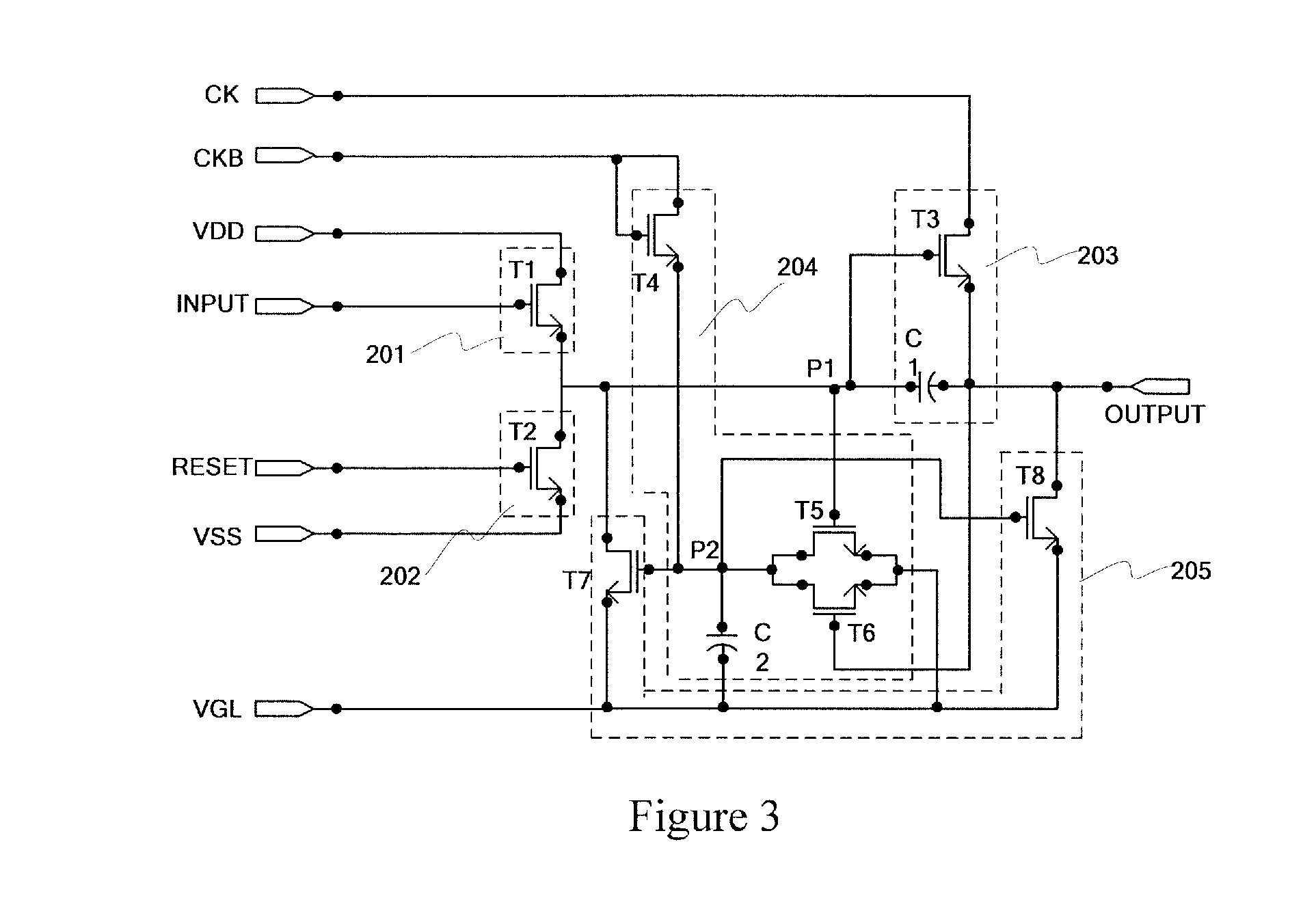
[0046]According to the present disclosure, there is provided a shift register unit, and its structure is as shown in FIG. 3. It can be seen from FIG. 3 that the shift register unit also comprises the input module 201, the reset module 202, the output module 203, the pull-down control module 204 and the pull-down module 205. The shift register unit as shown in FIG. 3 differs from the shift register unit as shown in FIG. 2 in:

[0047]in the shift register unit as shown in FIG. 3, the pull-down control module 204 further comprises a second capacitor C2 connected between the second node P2 and the power supply negative voltage terminal VGL, is configured to keep a high potential after an output of the output terminal OUTPUT; if there is no the second capacitor C2, the shift register unit as shown in FIG. 2 can also keep the high potential depending on a parasitic capacitor of the thin film transistor. However, there is a leakage current in the fifth thin film transistor T5 and the sixth t...

third embodiment

[0048]The above shift register units are connected in cascade to form an array substrate gate driving circuit. According to the present disclosure, there is provided a gate driving circuit, comprising respective stages of the shift register units connected in cascade, wherein an input signal terminal of a first stage of shift register unit is connected to a start signal terminal, and a reset signal terminal thereof is connected to an output terminal of a second stage of shift register unit; an input signal terminal of a last stage of shift register unit is connected to an output terminal of a previous stage of shift register unit, and a reset signal terminal thereof is connected to the start signal terminal.

[0049]Except for the first and the last stages of shift register units, an input signal terminal of each of the remaining stages of shift register units is connected to the output terminal of the previous stage of shift register unit, and a reset signal terminal thereof is connec...


PUM


Abstract

The present disclosure relates to the technical field of communication. There is provided a shift register unit and a gate driving circuit for decreasing noise interferences, enhancing stability of the shift register unit, and at the same reducing the size of the shift register unit. The shift register unit comprises: an input module configured to provide a first voltage signal to an output terminal in response to an input signal; a reset module configured to provide a second voltage signal to a first node as an output terminal of the input module in the input module in response to a reset signal; an output module configured to provide a first clock signal to the output terminal in response to a voltage at a first node; a pull-down control module configured to provide a second clock signal to a second node in response to the second clock signal and provide a power supply negative voltage to the second node in response to the voltage at the first node or the voltage at the output terminal; and a pull-down module configured to provide the power supply negative voltage to the first node and the output terminal in response to the voltage at the second node.

Description

TECHNICAL FIELD[0001]The present disclosure relates to the technical field of communication, in particular to a shift register unit and a gate driving circuit.BACKGROUND[0002]A thin film transistor liquid crystal display (TFT-LCD) driver mainly comprises a gate driver and a data driver, wherein the gate driver applies an input clock signal transformed by a shift register unit to a gate line of a liquid crystal display panel. A gate driving circuit can have the same process as the forming of TFT and form on the LCD panel together with the TFT simultaneously. The gate driving circuit comprises multiple stages of shift register units, each of which is connected to a corresponding gate line to output a gate driving signal. Respective stages of the gate driving circuit are connected with each other. A start signal is inputted to a first stage of the respective stages and the gate driving signal is sequentially outputted to the gate line, wherein an input terminal of a present stage is co...

Claims


Application Information

Patent Timeline
Patent Type & Authority Applications(United States)
IPC IPC(8): G11C19/28G09G3/36
CPCG11C19/28G09G2300/04G09G2310/08G09G3/3648G09G3/3674G09G2310/0286
Inventor LI, FUQIANGLI, CHENGAN, SEONG JUN
Owner BOE TECH GRP CO LTD
Why Eureka
Try Eureka