
Spin-On Layer for Directed Self Assembly with Tunable Neutrality

a technology of tunable neutrality and spin-on layer, which is applied in the direction of photomechanical equipment, instruments, and photosensitive material processing, etc., can solve the problems of insufficiently small holes, trenches, and lines in the pattern developed from photoresists, and achieve efficient, directed self-assembly

Active Publication Date: 2016-09-22
TOKYO ELECTRON LTD
View PDF7 Cites 9 Cited by
  • Summary
  • Abstract
  • Description
  • Claims
  • Application Information

AI Technical Summary

Benefits of technology

The patent text describes a method for modifying layers of materials on a substrate to create a more neutral surface that allows for more efficient self-assembly. Using a polymer system and a chemical reaction, the surface energy of the polymer can be altered to match the energy of a specific block co-polymer system. This allows for the creation of desired morphologies during self-assembly. The technical effect is an improved ability to create highly organized and efficient patterns on surfaces using polymer systems.

Problems solved by technology

Currently there are challenges with using lithographic tools to create patterns having critical dimensions to meet design specifications.
In other words, due to the resolution limitations of patterning photoresists, patterns developed from photoresists do not have lines, trenches, and holes that are sufficiently small to meet design specifications.
One challenge with spin-on neutral layers is that they are typically specifically tuned to a fixed DSA chemistry in terms of composition of the individual blocks, the relative percent of one block to another, and the overall molecular weight of the block co-polymer.

Method used


Image

  • Spin-On Layer for Directed Self Assembly with Tunable Neutrality
  • Spin-On Layer for Directed Self Assembly with Tunable Neutrality
  • Spin-On Layer for Directed Self Assembly with Tunable Neutrality

Examples


Embodiment Construction

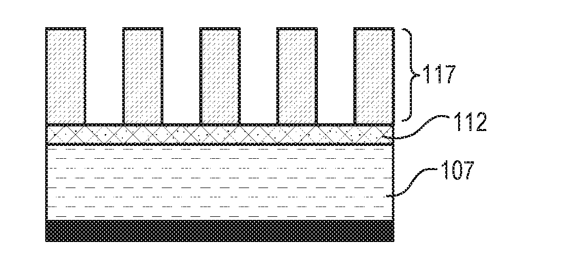
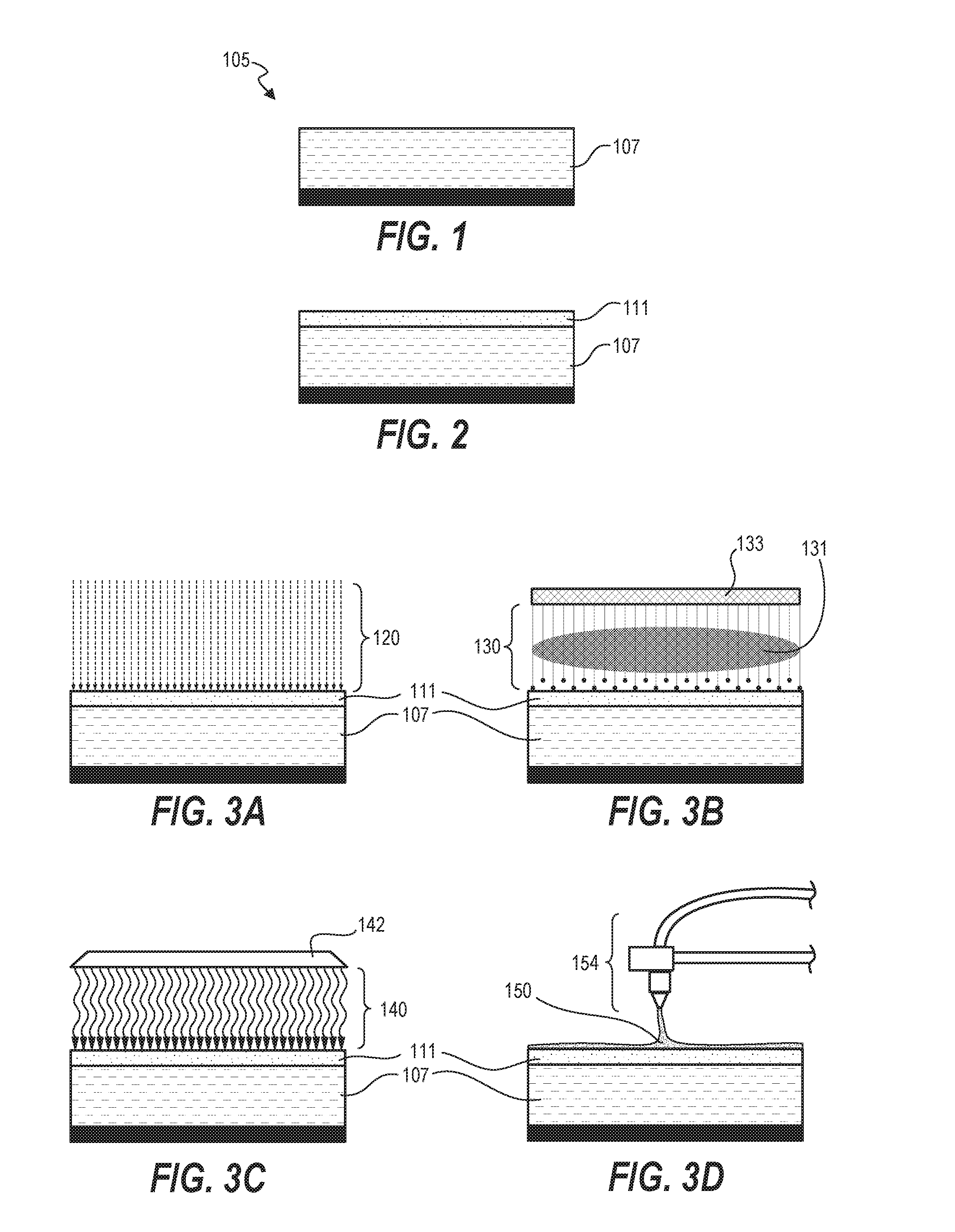
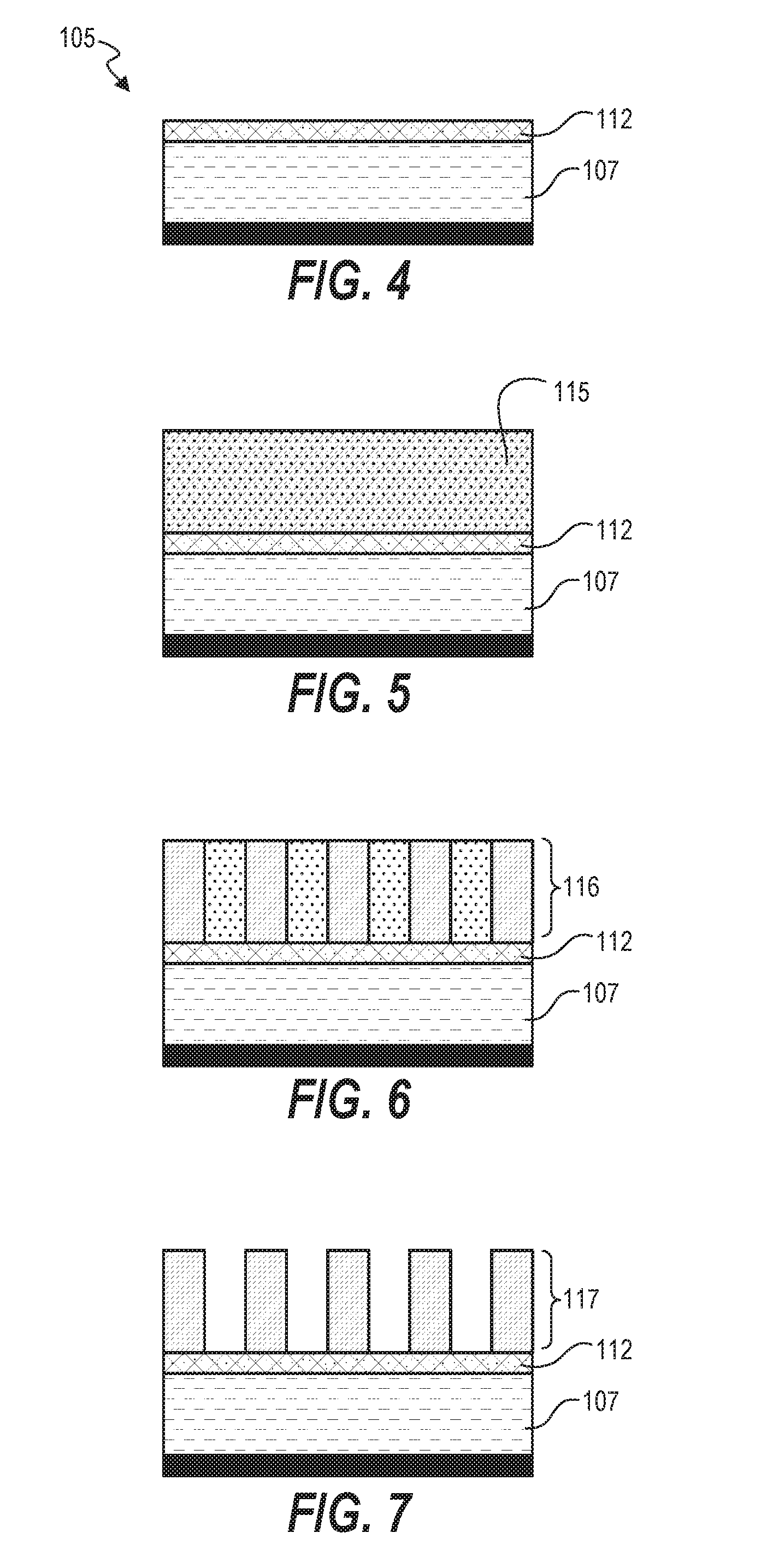
[0022]Successful directed self-assembly of block copolymers is realized when self-assembled on a neutral layer. This neutral layer matches (in characteristics) the directed self-assembly material to be applied on top of the neutral layer. Conventionally, there is no generic neutral layer that is compatible with multiple different block copolymer materials. Techniques disclosed herein include methods for creating a directed self-assembly tunable neutral layer that works with multiple different block copolymer materials. Techniques herein can include depositing a neutral layer and then post-processing this neutral layer to tune its characteristics so that the neutral layer is compatible with a particular block copolymer scheme or schemes. Post-processing herein of such a neutral layer can modify a ratio of pi and sigma bonds in a given carbon film or other film to approximate a given self-assembly film that will be deposited on this neutral layer.

[0023]Techniques herein include treati...


PUM

PropertyMeasurementUnit
wavelengthaaaaaaaaaa
wavelengthsaaaaaaaaaa

Abstract

Techniques disclosed herein include methods for creating a directed self-assembly tunable neutral layer that works with multiple different block copolymer materials. Techniques herein can include depositing a neutral layer and then post-processing this neutral layer to tune its characteristics so that the neutral layer is compatible with a particular block copolymer scheme or schemes. Post-processing herein of such a neutral layer can modify a ratio of pi and sigma bonds in a given carbon film or other film to approximate a given self-assembly film that will be deposited on this neutral layer. Accordingly, a generic or single material can be used for a neutral layer and modified to match a given block copolymer to be deposited.

Description

CROSS REFERENCE TO RELATED APPLICATIONS[0001]The present application claims the benefit of U.S. Provisional Patent Application No. 62 / 134,149, filed on Mar. 17, 2015, entitled “Spin-On Under Layer for Directed Self Assembly with Tunable Neutrality,” which is incorporated herein by reference in its entirety.BACKGROUND OF THE INVENTION[0002]Techniques herein relate to methods of fabricating semiconductors including methods for patterning substrates.[0003]Fabricating semiconductors includes patterning a wafer surface to be able to create various trenches, holes, and openings in underlying layers. Currently there are challenges with using lithographic tools to create patterns having critical dimensions to meet design specifications. In other words, due to the resolution limitations of patterning photoresists, patterns developed from photoresists do not have lines, trenches, and holes that are sufficiently small to meet design specifications. One technique to shrink patterns to desired d...

Claims


Application Information

Patent Timeline
Patent Type & Authority Applications(United States)
IPC IPC(8): H01L21/027G03F7/20G03F7/16
CPCH01L21/0279H01L21/0274G03F7/2059G03F7/16H01L21/0277H01L21/0271H01L21/31058G03F7/0002G03F7/002G03F7/004G03F7/11G03F7/165G03F7/265G03F7/40H01L21/3081H01L21/3086G03F7/26C09D153/00H01L21/0337C08L53/00B81C2201/0149B82Y30/00
Inventor SMITH, JEFFREY
Owner TOKYO ELECTRON LTD
Learn More