Selective segment via plating process and structure

Active Publication Date: 2016-09-22
MULTEK TECH LTD
View PDF7 Cites 14 Cited by
  • Summary
  • Abstract
  • Description
  • Claims
  • Application Information

AI Technical Summary

Benefits of technology

[0014]In some embodiments, the method also includes pattern etching the conductive layers in the laminated stack. In some embodiments, the via wall plating forms electrical interconnections with conductive layers intersecting the via, and second via wall plating discontinuities electrically isolate a first segment of electrically interconnected conductive layers from a second segment of electrically interconnected conductive layers. In some embodiments, performing the electroplating process comprises applying electricity to the first segment and to the second segment. In some embodiments, the first plating resist layer prevents formation of a plating

Problems solved by technology

Stripping of the electroless plating on the plating res

Method used


Image

  • Selective segment via plating process and structure
  • Selective segment via plating process and structure
  • Selective segment via plating process and structure

Examples


Example

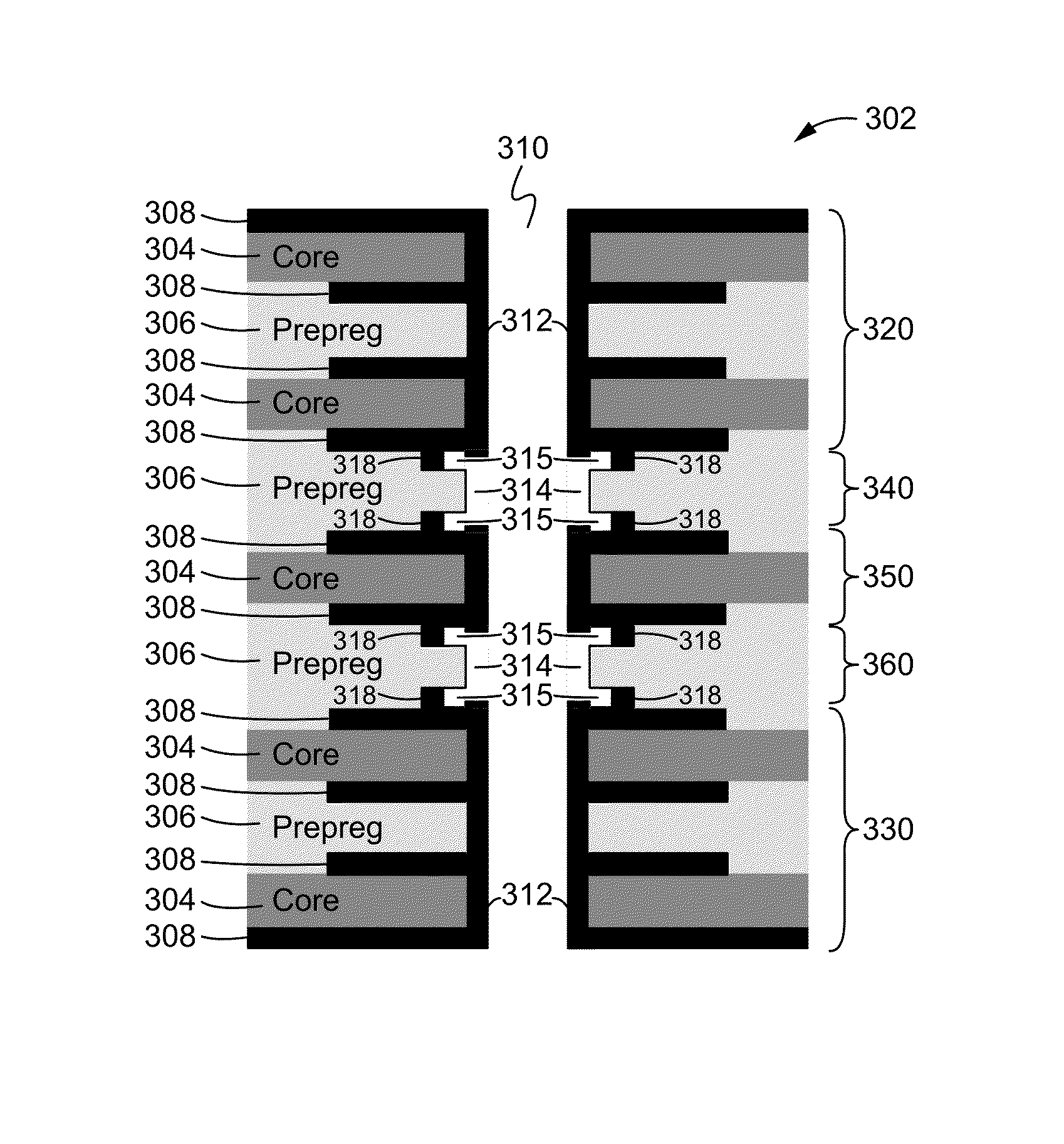
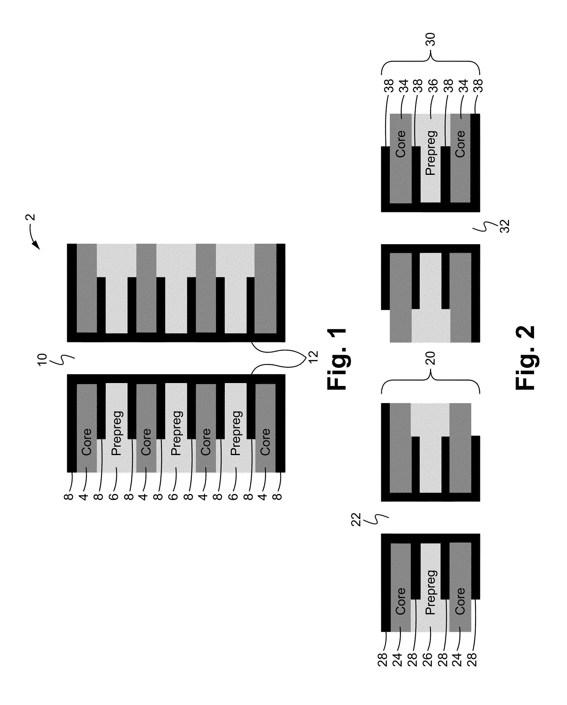
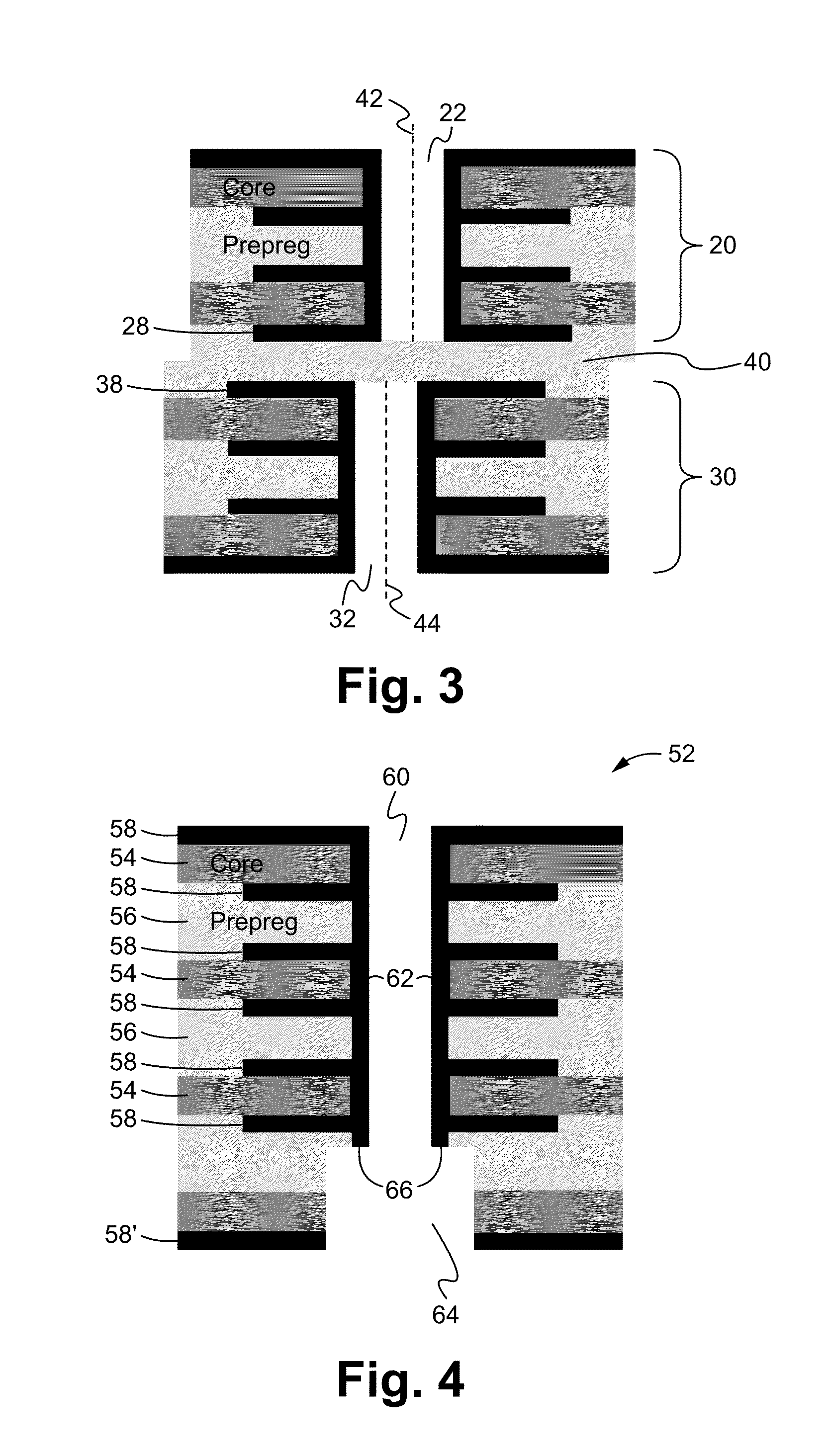
[0026]Embodiments of the present application are directed to a printed circuit board. Those of ordinary skill in the art will realize that the following detailed description of the printed circuit board is illustrative only and is not intended to be in any way limiting. Other embodiments of the printed circuit board will readily suggest themselves to such skilled persons having the benefit of this disclosure.

[0027]Reference will now be made in detail to implementations of the printed circuit board as illustrated in the accompanying drawings. The same reference indicators will be used throughout the drawings and the following detailed description to refer to the same or like parts. In the interest of clarity, not all of the routine features of the implementations described herein are shown and described. It will, of course, be appreciated that in the development of any such actual implementation, numerous implementation-specific decisions must be made in order to achieve the develope...


PUM


Abstract

A selective segment via plating process for manufacturing a circuit board selectively interconnects inner conductive layers as separate segments within the same via. Plating resist is applied to a conductive layer of an inner core and then stripped off after an electroless plating process. Stripping of the electroless plating on the plating resist results in a plating discontinuity on the via wall. In a subsequent electroplating process, the plug non-conductive layer can not be plated due to the plating discontinuity. The resulting circuit board structure has separate electrically interconnected segments within the via.

Description

CROSS-REFERENCE TO RELATED APPLICATION(S)[0001]This application claims priority under 35 U.S.C. §119(a)-(d) of the Chinese Patent Application No: 201510127856.X, filed Mar. 23, 2015 and titled, “SELECTIVE SEGMENT VIA PLATING PROCESS AND STRUCTURE,” and the Chinese Patent Application No: 201510121886.X, filed Mar. 19, 2015 and titled, “SELECTIVE SEGMENT VIA PLATING PROCESS AND STRUCTURE,” which are both hereby incorporated by reference in their entireties for all purposes.FIELD OF THE INVENTION[0002]The present invention is generally directed to printed circuit boards. More specifically, the present invention is directed to printed circuit boards having selective segment via plating.BACKGROUND OF THE INVENTION[0003]A printed circuit board (PCB) mechanically supports and electrically connects electronic components using conductive traces, pads and other features etched from electrically conductive sheets, such as copper sheets, laminated onto a non-conductive substrate. Multi-layered ...

Claims


Application Information

Patent Timeline
IPC IPC(8): H05K1/11H05K3/46H05K3/42H05K1/02H05K3/00
CPCH05K1/115H05K1/0298H05K3/0047H05K3/422H05K2201/10303H05K3/429H05K3/4611H05K3/4638H05K2201/09545H05K3/424H05K1/0216H05K1/112H05K3/0058H05K3/06H05K3/181H05K3/188H05K3/42H05K3/4602H05K3/4623H05K2201/095H05K2201/09554
Inventor PEN, KWANYU, PUI YIN
Owner MULTEK TECH LTD
Why Eureka
Try Eureka