Integrated laser with back-reflection isolator

a back-reflection isolator and integrated laser technology, applied in the field of optical coupling optical signals, can solve the problems of low-cost and reliable array laser sources integrated with silicon photonics that cannot be implemented large-scale integrated silicon photonics, and the difficulty of low-cost and reliable array laser sources integrated with silicon photonics, so as to reduce the back reflection of optical signals

Active Publication Date: 2016-10-06
ORACLE INT CORP
View PDF5 Cites 41 Cited by
  • Summary
  • Abstract
  • Description
  • Claims
  • Application Information

AI Technical Summary

Benefits of technology

[0013]One embodiment of the present disclosure provides an integrated circuit. This integrated circuit includes: a substrate; a buried-oxide (BOX) layer disposed on the substrate; and a semiconductor layer disposed on the BOX layer, where the semiconductor layer includes an optical coupler and an optical waveguide. Moreover, the integrated circuit includes: an isolator disposed on the semiconductor layer; and an optical source, disposed on the isolator, which includes a lens. During operation, the optical source generates an optical signal that propagates toward the isolator so that the lens focuses the optical signal. Furthermore, during operation the isolator reduces back reflection of the optical signal toward the optical source, and the optical coupler couples the optical signal into the optical waveguide.

Problems solved by technology

However, because of thermal constraints and other physical limits, the performance scaling of such large-scale integrated circuits may not be associated with increased clock rates.
However, low-cost and reliable array laser sources integrated with silicon photonics remain an obstacle to implementing large-scale integrated silicon photonic links
While individual external III-V laser sources are commercially available, low-cost integration of an array of external laser sources onto a silicon photonics chip remains a challenge.
However, in practice this approach is prohibitively expensive.
However, the yield and reliability of this distributed feedback laser remain obstacles to low-cost optical sources.
Moreover, III-V materials and processes are usually not defect-free.
Furthermore, burn-in is also typically required to weed out the infant failures.
Therefore, it is not typically ideal to integrate III-V lasers with silicon photonics circuits before component qualification, especially for applications such as large bandwidth system interconnects in which large integration scale is typically required.
However, the scaling of such an optical source is often limited given the limited maximum power of an individual laser die.
Moreover, integration of many laser packages onto a single silicon photonics chip may be needed for large bandwidth system interconnects, such as applications with tens and hundreds of optical links, which represents a significant challenge for packaging and integration.

Method used


Image

  • Integrated laser with back-reflection isolator
  • Integrated laser with back-reflection isolator
  • Integrated laser with back-reflection isolator

Examples


Embodiment Construction

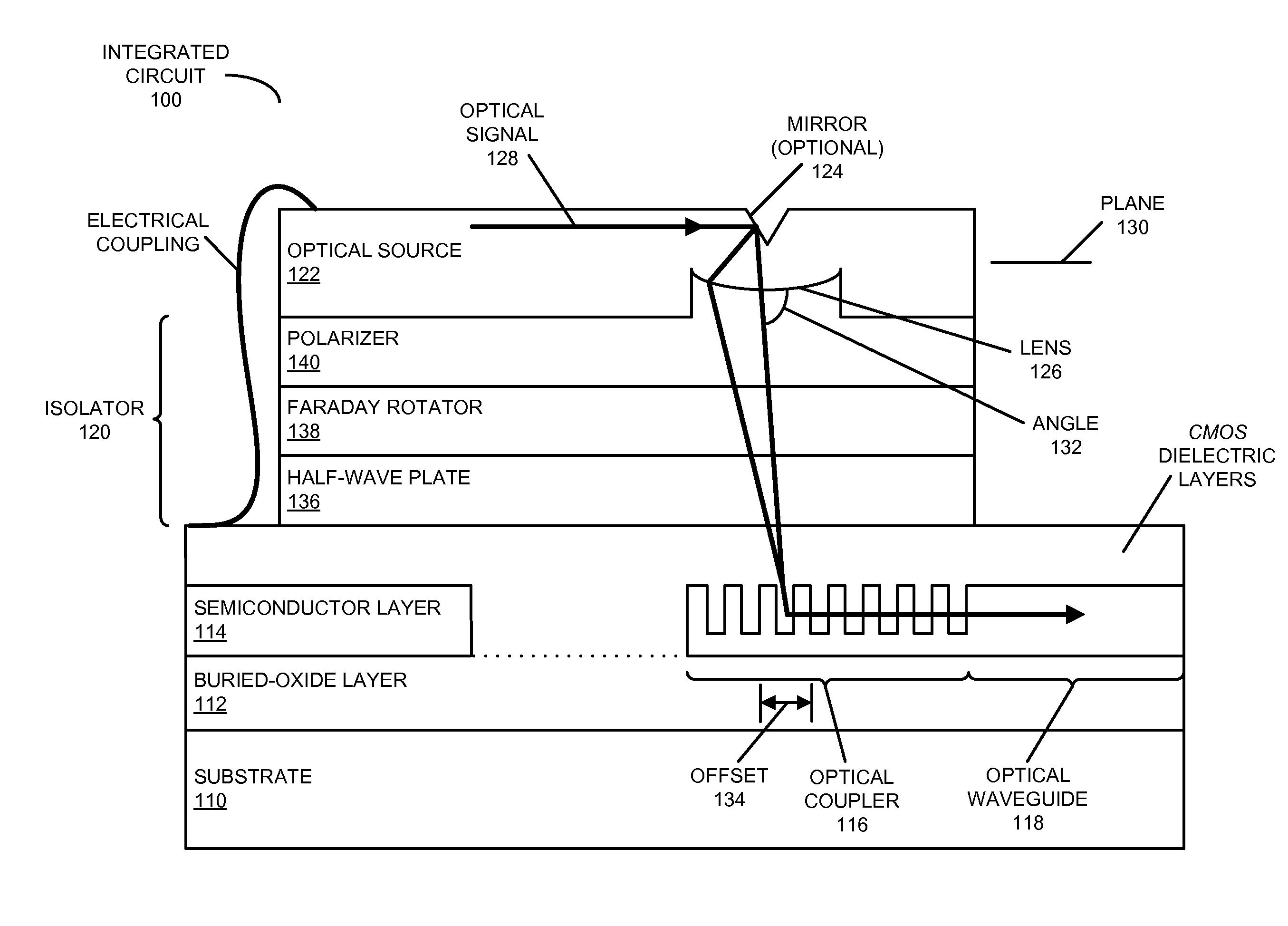
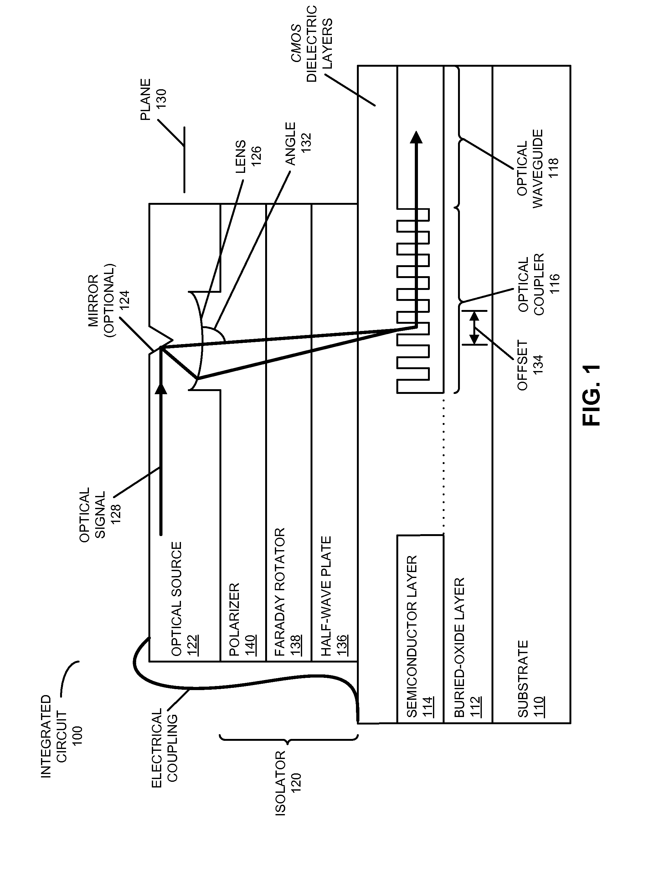
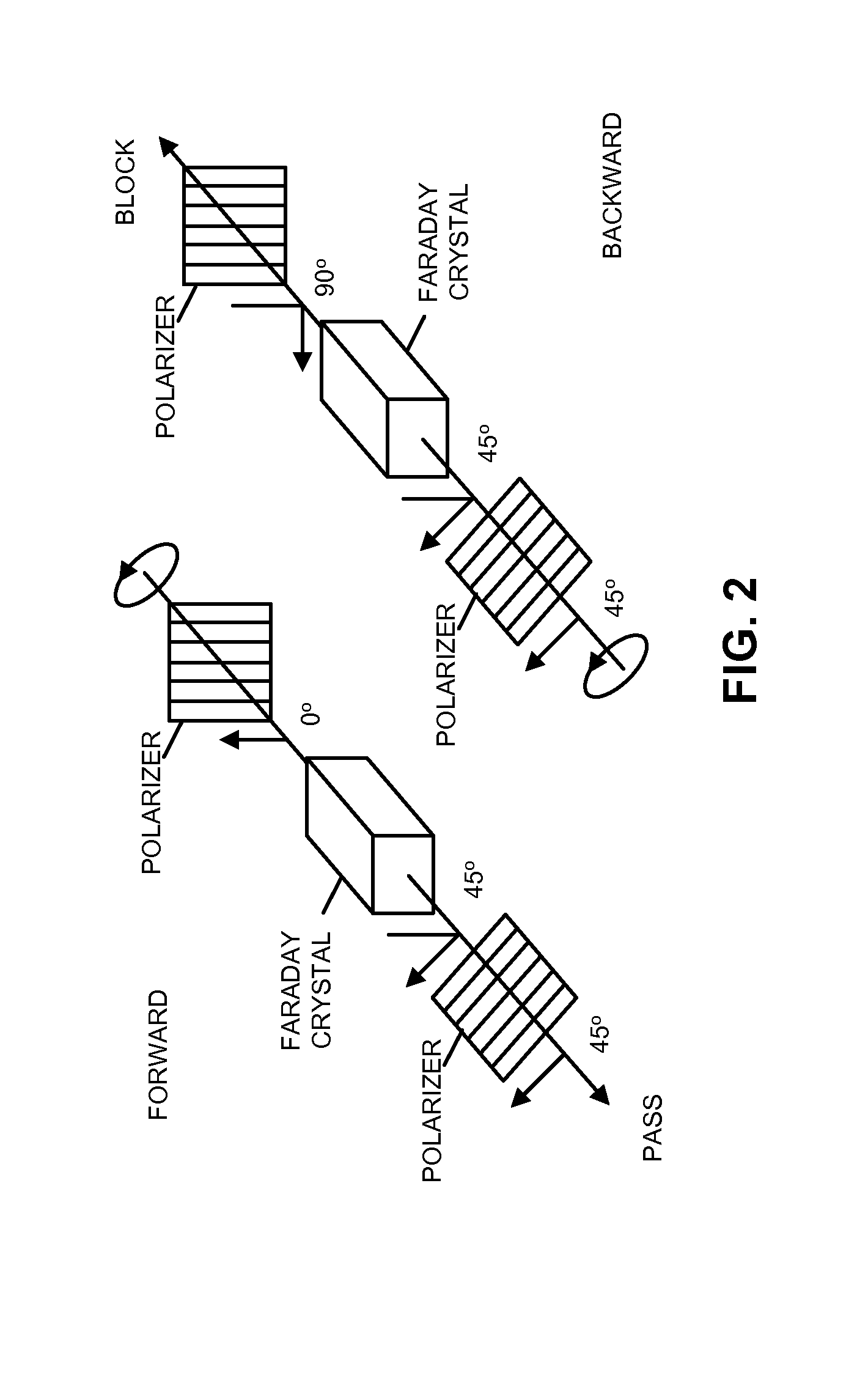
[0027]Embodiments of an integrated circuit that includes an optical source, a system that includes the integrated circuit, and a method for optically coupling an optical signal into an optical waveguide are described. The integrated circuit includes an optical source (such as a laser) and a lens, which is disposed on an isolator. Moreover, the isolator is disposed on a semiconductor layer in a silicon-on-insulator (SOI) platform that includes an optical coupler and an optical waveguide. During operation, the optical source generates an optical signal so that the optical signal propagates toward the isolator, and the lens focuses the optical signal. Furthermore, the isolator reduces or eliminates back reflection of the optical signal toward the optical source, and the optical coupler couples the optical signal into the optical waveguide.

[0028]This optical integration technique may facilitate low-cost and high yield integration of a surface-normal coupled array laser source (SCALS) wi...


PUM


Abstract

An integrated circuit includes an optical source (such as a laser) with a lens, which is disposed on an isolator. This isolator is disposed on a semiconductor layer in a silicon-on-insulator (SOI) platform that includes an optical coupler and an optical waveguide. During operation, the optical source generates an optical signal that propagates toward the isolator so that the lens focuses the optical signal. Furthermore, the isolator reduces or eliminates back reflection of the optical signal toward the optical source, and the optical coupler couples the optical signal into the optical waveguide.

Description

CROSS REFERENCE TO RELATED APPLICATIONS[0001]This application claims priority under 35 U.S.C. §119(e) to: U.S. Provisional Application Ser. No. 62 / 141,721, entitled “Integrated Surface-Normal Coupled Array Laser Sources (SCALS) for Si Photonic Circuits,” by Xuezhe Zheng, Ashok V. Krishnamoorthy and Kannan Raj, Attorney Docket No. ORA15-0948-US-PSP, filed on Apr. 1, 2015; and U.S. Provisional Application Ser. No. 62 / 142,332, entitled “Integrated Surface-Normal Coupled Array Laser Sources (SCALS) for Si Photonic Circuits,” by Xuezhe Zheng, Ashok V. Krishnamoorthy and Kannan Raj, Attorney Docket No. ORA15-0948PSP2, filed on Apr. 2, 2015, the contents of both of which are herein incorporated by reference.GOVERNMENT LICENSE RIGHTS[0002]This invention was made with U.S. Government support under Agreement No. HR0011-08-9-0001 awarded by DARPA. The U.S. Government has certain rights in the invention.BACKGROUND[0003]1. Field[0004]The present disclosure relates to techniques for optically cou...

Claims


Application Information

Patent Timeline
Patent Type & Authority Applications(United States)
IPC IPC(8): H01S5/022H01S5/026H01S5/185
CPCH01S5/026H01S5/0228G02B6/12004G02B6/124G02B6/42H01S5/021H01S5/0267G02B6/4208H01L2224/48091H01L2924/00014H01S5/0268H01S5/0225H01S5/185
Inventor ZHENG, XUEZHEKRISHNAMOORTHY, ASHOK V.RAJ, KANNAN
Owner ORACLE INT CORP
Why Eureka
Try Eureka