

PACKAGING SOLUTIONS FOR DEVICES AND SYSTEMS COMPRISING LATERAL GaN POWER TRANSISTORS
- Summary
- Abstract
- Description
- Claims
- Application Information
AI Technical Summary
Benefits of technology
Problems solved by technology
Method used
Image

Examples
first embodiment
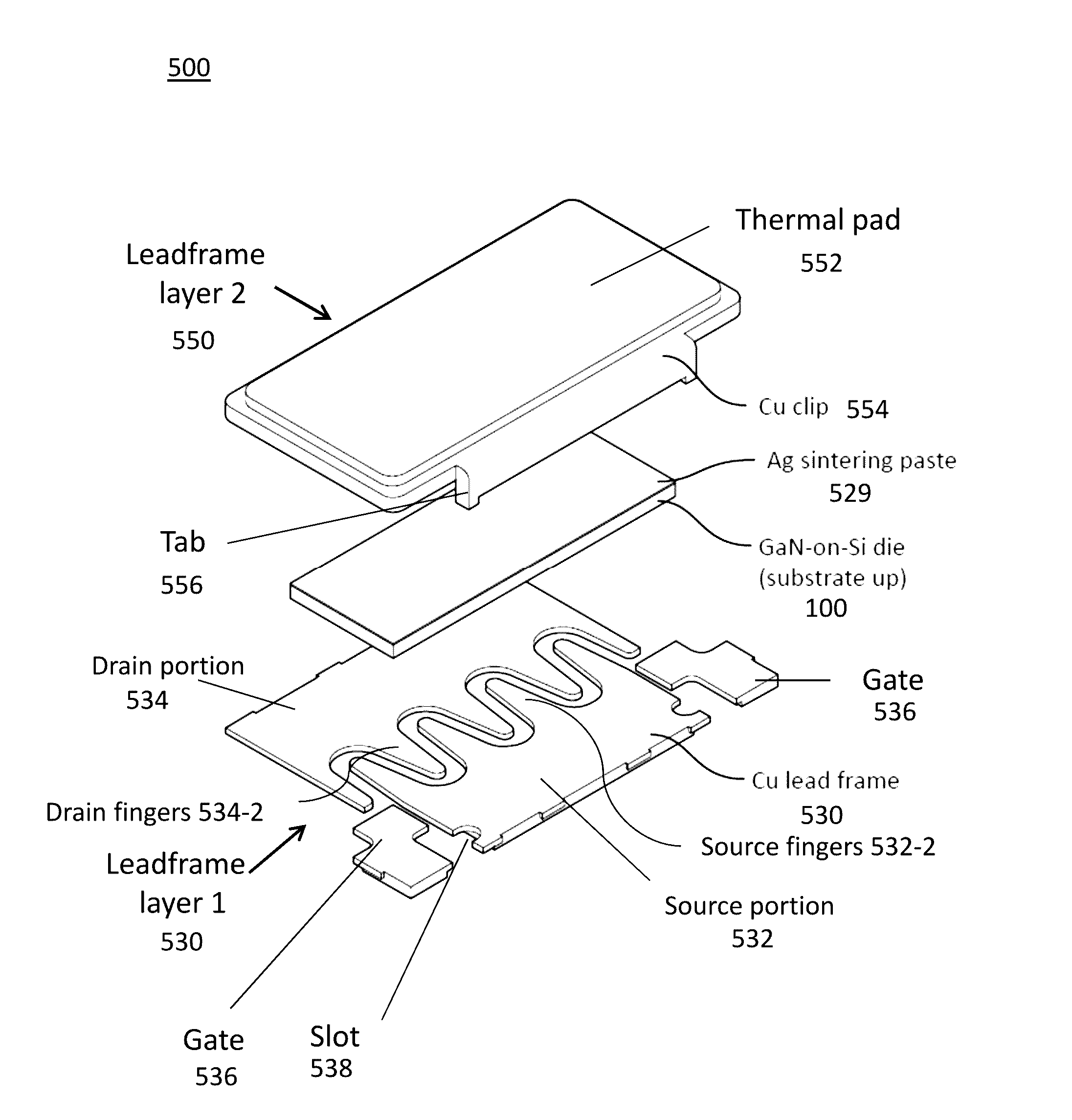
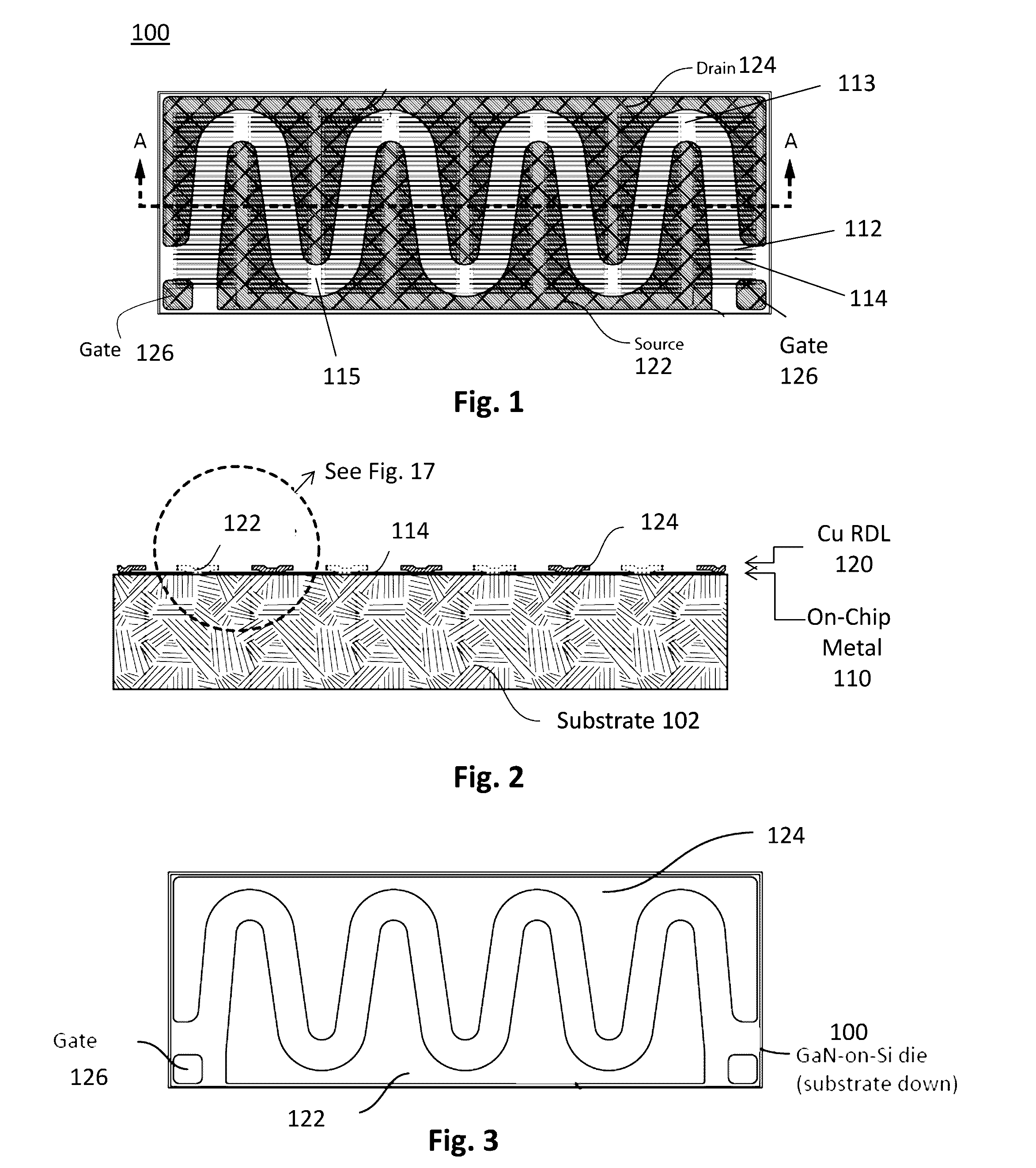
[0068]FIG. 7 shows a schematic exploded view of components of a packaging assembly 500 comprising a lateral GaN die 100, according to the present invention. The lateral GaN die 100 is flipped (substrate up) and sandwiched between first and second copper leadframe layers 530 and 550. The first leadframe layer 530 is a patterned copper leadframe having a source portion 532, a drain portion 534 and gate portions 536, respectively. The second leadframe 550 comprises an area forming a thermal pad 552, and also provides a source clip 554, which extends laterally and downwards to provide for a vertical connection to the corresponding source portion 532 of the first copper leadframe layer 530. By way of example, in this embodiment, the first copper leadframe layer is patterned to form source, drain and gate portions that are arranged to match, or correspond to, the arrangement of source, drain and gate contact areas of the GaN die shown in FIG. 3, and which extend laterally of the GaN die. ...
fourth embodiment
[0081]A method of fabrication of a packaging assembly of the fourth embodiment, comprising a GaN die 100, a first leadframe layer 830 and a second leadframe layer 850 is illustrated schematically in FIGS. 22A to 22F. The GaN die is provided with a front surface providing source, drain and gate contact areas for the lateral GaN power transistor and a back surface for die-attach, for example, as illustrated in FIGS. 1 to 3. The first leadframe layer comprises source, drain and gate portions for interconnection to respective source, drain and gate contact areas of the lateral GaN power transistor. Optionally, the first leadframe layer comprises a support frame 831 (indicated by dotted lines) that surrounds and holds together the source, drain and gate portions during assembly. The second leadframe layer provides a thermal pad and a die-attach area for the back surface of the GaN die, e.g. as illustrated in FIG. 21 and acts as a source clip. The GaN die is positioned relative to the fir...
PUM
 Abstract
Description
Claims
Application Information