A copper-tin-copper bonding process and structure based on copper nanorods

A technology of copper nanorods and copper bonding, which is applied in the direction of nanotechnology, nanotechnology, nanotechnology, etc. for materials and surface science, can solve the problems of reducing interconnection temperature, reduce thermal deformation and thermal stress, and improve Bond quality, highly controllable results

Active Publication Date: 2019-01-15
HUAZHONG UNIV OF SCI & TECH
View PDF6 Cites 0 Cited by
  • Summary
  • Abstract
  • Description
  • Claims
  • Application Information

AI Technical Summary

Problems solved by technology

However, the current bonding temperature of this technology is generally 260-320°C, which is slightly higher than the melting point of tin. How to improve this technology to further reduce the interconnection temperature and the requirements for the bonding environment is still a challenge

Method used


Image

  • A copper-tin-copper bonding process and structure based on copper nanorods
  • A copper-tin-copper bonding process and structure based on copper nanorods
  • A copper-tin-copper bonding process and structure based on copper nanorods

Examples


Embodiment 1

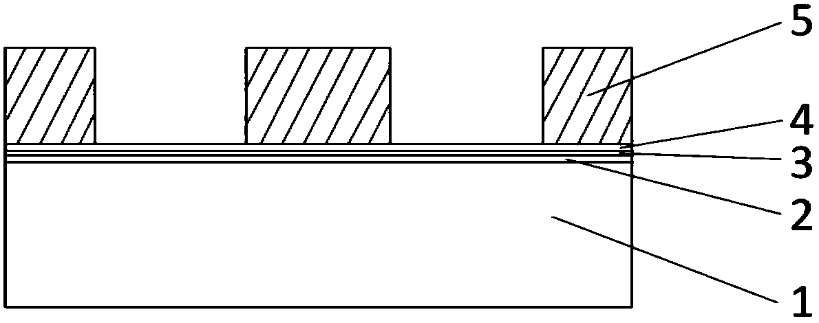
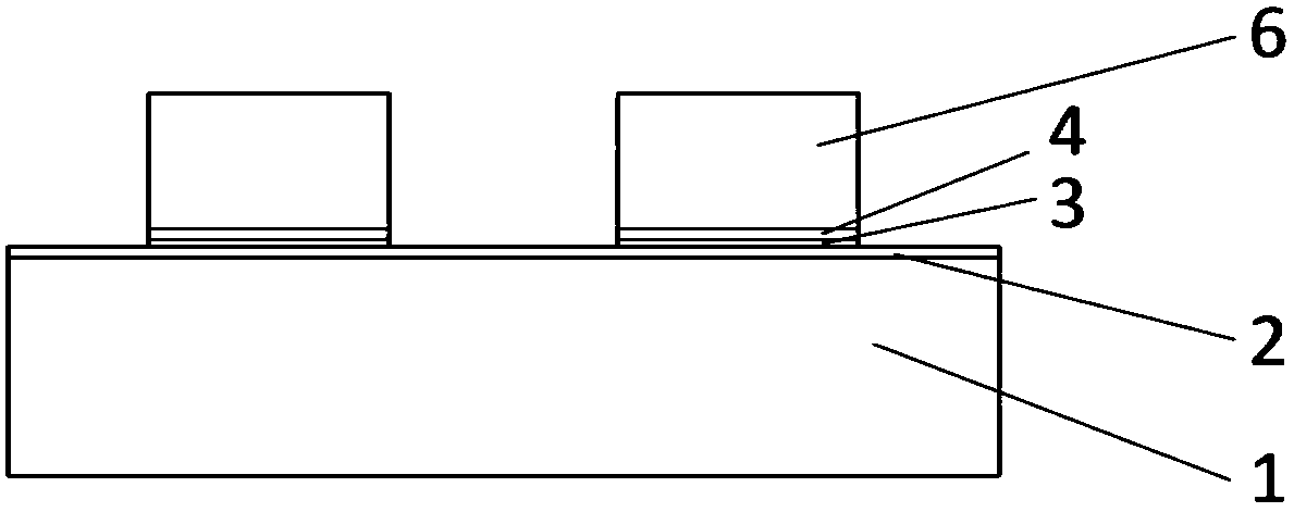
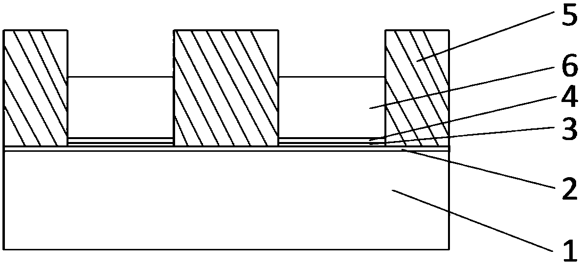
[0061] The copper-tin-copper bonding process based on copper nanorods includes the following steps:

[0062] (1) Deposit a layer of insulating layer SiO on the clean substrate surface by thermal oxidation 2 , with a thickness of 50nm; and then using magnetron sputtering to sequentially deposit an adhesion layer Ti and a seed layer Cu with a thickness of 20nm and 50nm, respectively.

[0063] (2) Spin-coat PR1-4000A positive photoresist with a thickness of 5 μm on the surface of the seed layer, use a pattern mask containing an area-array circular hole, the circular hole area is transparent, the diameter of the circular hole is 5 μm, and the center distance of the circular hole 10 μm, use MA6 contact photolithography machine for photolithography, and use RD6 developer for development, rinse with deionized water and blow dry with nitrogen gun.

[0064] (3) Put the pattern obtained by photolithography into the copper plating solution for electroplating. The copper plating solution...

Embodiment 2

[0070] The copper-tin-copper bonding process based on copper nanorods includes the following steps:

[0071] (1) Deposit a layer of insulating layer SiO on the clean substrate surface by thermal oxidation 2 , with a thickness of 50nm; then, the adhesion layer TiW and the seed layer Cu are sequentially deposited by magnetron sputtering, with thicknesses of 50nm and 100nm, respectively.

[0072] (2) Spin-coat PR1-12000A positive photoresist with a thickness of 20 μm on the surface of the seed layer, use a pattern mask containing an area array hole, the hole area is transparent, the diameter of the hole is 50 μm, and the center distance of the hole 100 μm, use MA6 contact photolithography machine for photolithography, and use RD6 developer for development, rinse with deionized water and blow dry with nitrogen gun.

[0073] (3) Put the pattern obtained by photolithography into the copper plating solution for electroplating. The copper plating solution selects SYSB2210 bump copper...

Embodiment 3

[0079] The copper-tin-copper bonding process based on copper nanorods includes the following steps:

[0080] (1) Deposit a layer of insulating layer Si on the clean substrate surface by chemical vapor deposition (CVD) 3 N 4 , with a thickness of 100 nm; then, an adhesion layer Ti and a seed layer Cu are sequentially deposited by magnetron sputtering, with thicknesses of 50 nm and 200 nm, respectively.

[0081](2) Spin-coat NR26-25000P negative photoresist with a thickness of 50 μm on the surface of the seed layer, using a pattern mask containing a round hole around the hole, the hole area is opaque, the diameter of the hole is 100 μm, and the center of the hole is The distance is 400 μm, and the MA6 contact photolithography machine is used for photolithography, and the RD6 developer is used for development, and then rinsed with deionized water and blown dry with a nitrogen gun.

[0082] (3) Put the pattern obtained by photolithography into the copper plating solution for ele...


PUM

PropertyMeasurementUnit
diameteraaaaaaaaaa
diameteraaaaaaaaaa
diameteraaaaaaaaaa

Abstract

The invention discloses a copper nanorod based copper-tin-copper bonding process and structure. The process comprises the following steps of sequentially depositing an insulation layer, an adhesion layer and a seed layer on the surface of a substrate; spin-coating a layer of photoresist on the seed layer, and fabricating round holes in the photoresist; electroplating copper in the round holes to obtain copper convex points; removing the photoresist, and removing the exposed seed layer and the exposed adhesive layer; spin-coating the photoresist on the surfaces and the peripheries of the copper convex points, and exposing the upper surfaces of the copper convex points; electroplating tin convex points on the copper convex points of one of two substrate units obtained according to the above steps, and removing the photoresist; depositing copper nanorods on the copper convex points of the other substrate unit, and removing the photoresist; and bonding the two substrate units by a hot-pressing mode. The copper-tin-copper bonding structure is acquired according to the bonding process. According to the bonding process and the bonding structure, the copper nanorods are applied to copper-tin-copper bonding, the bonding temperature can be effectively reduced, and a tight bonding surface is obtained; and the preparation process is simple and controllable, is low in cost, and has great application value.

Description

technical field [0001] The invention belongs to the technical field of micro-nano manufacturing, and more specifically relates to a copper-tin-copper bonding process and structure based on copper nanorods. Background technique [0002] The sustained and rapid development of integrated circuits (ICs) has continuously triggered changes in products in various fields and created new social needs, playing a key supporting role in important fields such as national security, high-end manufacturing, and network communications. As the feature size enters the 20 / 14nm technology node, the technology route of the front-end process of IC manufacturing with extreme ultraviolet lithography as the main body has become clear, and a large number of dense interconnection micro-channels have emerged, triggering the interconnection and packaging technology in the back-end Three-dimensional integration has become an inevitable choice to improve device performance and cost performance. [0003] T...

Claims


Application Information

Patent Timeline
Patent Type & Authority Patents(China)
IPC IPC(8): H01L21/48H01L21/603H01L23/498B82Y30/00B82Y40/00
CPCB82Y30/00B82Y40/00H01L21/4853H01L23/49816H01L23/49866H01L24/81H01L2224/81359H01L2224/81895H01L2924/01029H01L2924/0105H01L2224/11H01L2224/81
Inventor 廖广兰独莉史铁林汤自荣陈鹏飞沈俊杰邵杰
Owner HUAZHONG UNIV OF SCI & TECH
Why Eureka
Try Eureka