Metal substrate and method of manufacturing the same

a metal substrate and metal technology, applied in the field of electromechanical circuit substrates, can solve the problems of increasing product defect rate, affecting production yield and dimensional stability, etc., and achieve the effects of preventing pad damage or delamination, enhancing structural strength of metal substrates, and increasing yield of printed circuit boards

Active Publication Date: 2016-10-27
AZOTEK
View PDF6 Cites 2 Cited by
  • Summary
  • Abstract
  • Description
  • Claims
  • Application Information

AI Technical Summary

Benefits of technology

The patent is about a way to make printed circuit boards using a double layer metal substrate. This increases the strength and prevents damage to the boards, which decreases defects and increases yield. The insulating substrate can be easily released from the metal layer without any residual adhesive, which means the metal layer can be separated and used to make two printed circuit boards. This increases efficiency and productivity of the printed circuit board process.

Problems solved by technology

However, fold damage, pad damage or delamination (or called as blistering) may occur in a single layer PI substrate for manufacturing an ultra-thin flexible printed circuit board during processing due to inadequate stiffness of the substrate, and thus to affect production yield and dimensional stability.
The adhesive may be remained during the reinforcing layer is tore off, which results in increasing of product defect rate.

Method used


Image

  • Metal substrate and method of manufacturing the same
  • Metal substrate and method of manufacturing the same
  • Metal substrate and method of manufacturing the same

Examples


Embodiment Construction

[0032]The following embodiments are disclosed with accompanying diagrams for detailed description. For illustration clarity, many details of practice are explained in the following descriptions. However, it should be understood that these details of practice do not intend to limit the present invention. That is, these details of practice are not necessary in parts of embodiments of the present invention. Furthermore, for simplifying the drawings, some of the conventional structures and elements are shown with schematic illustrations.

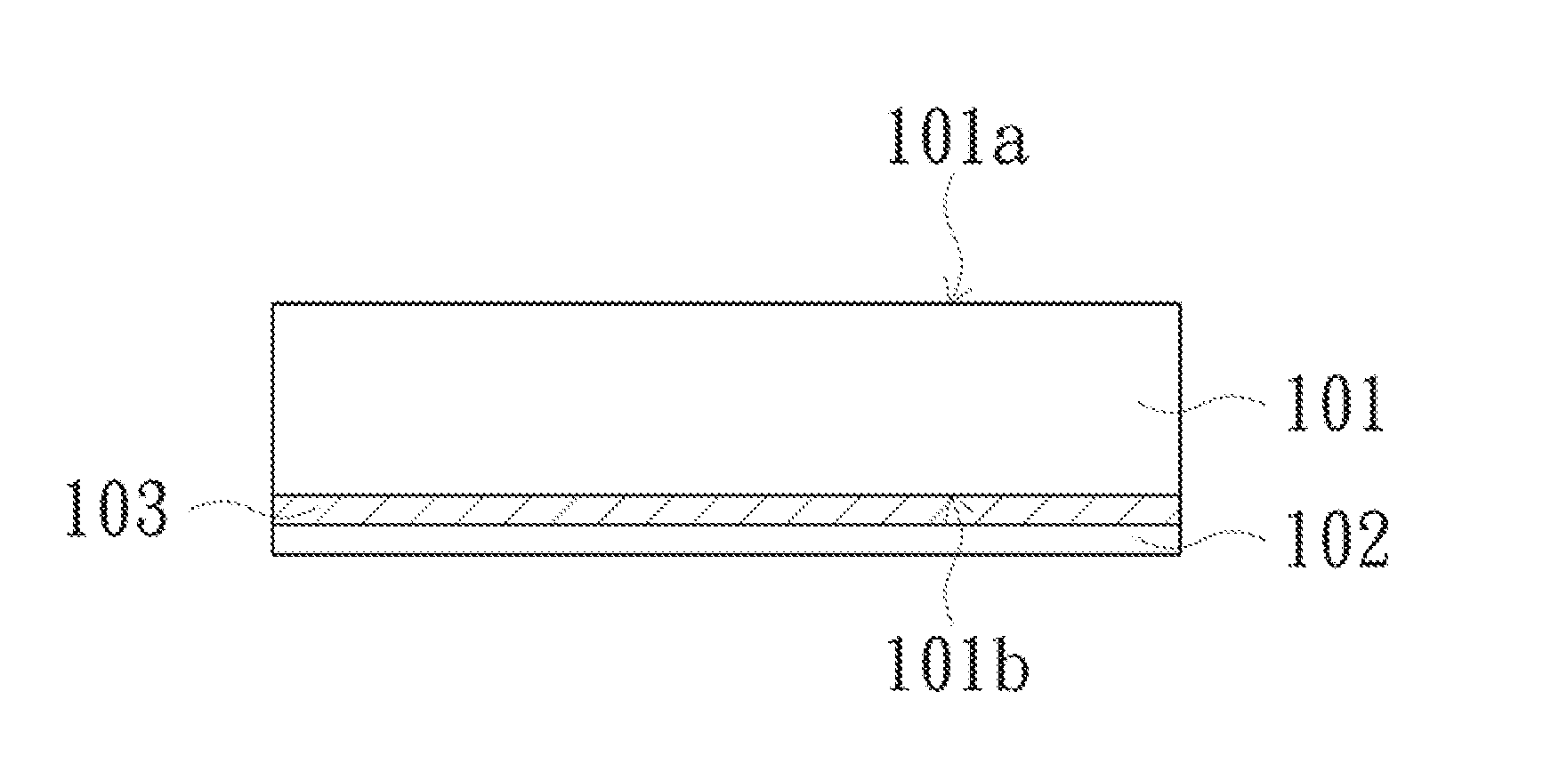
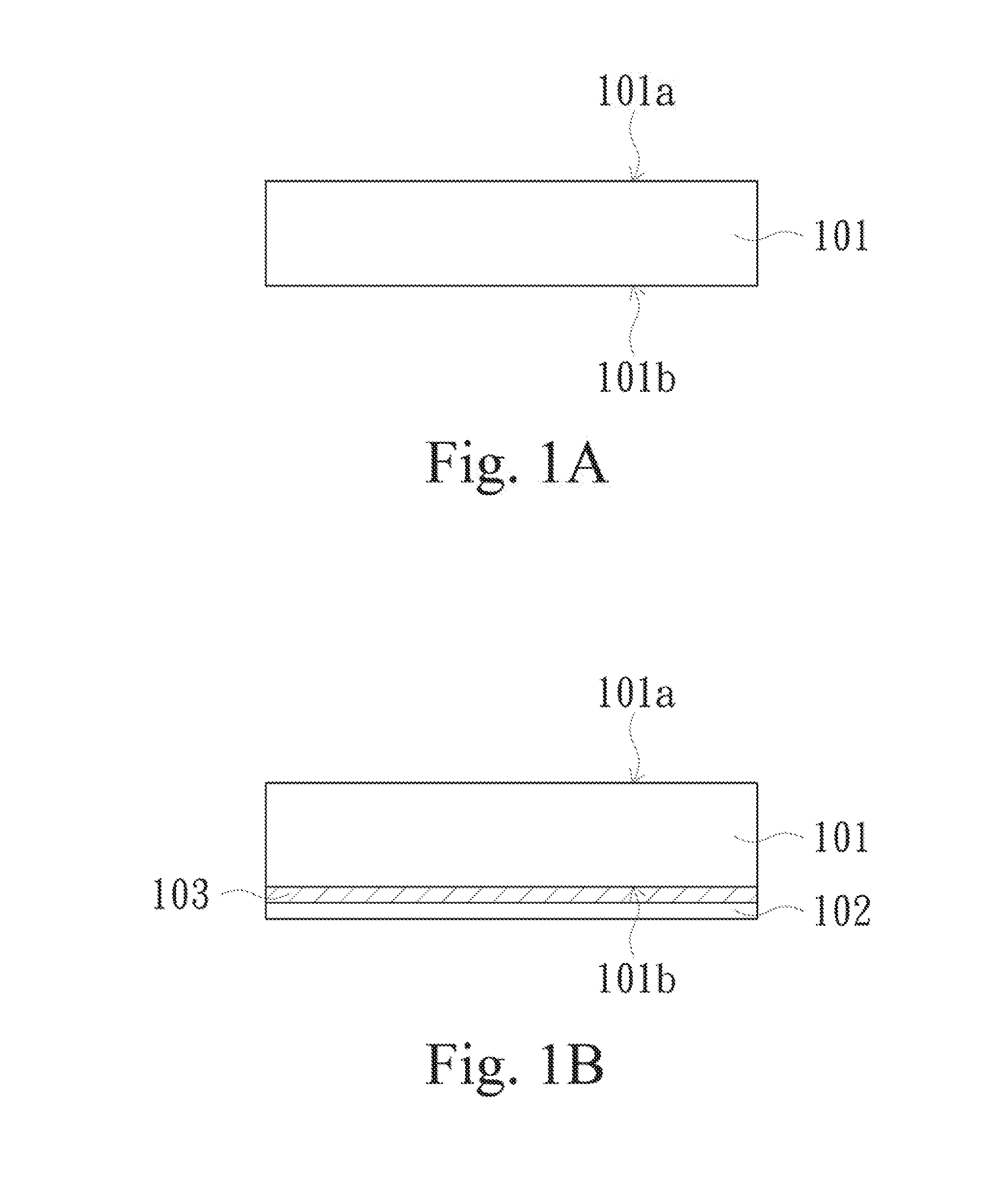
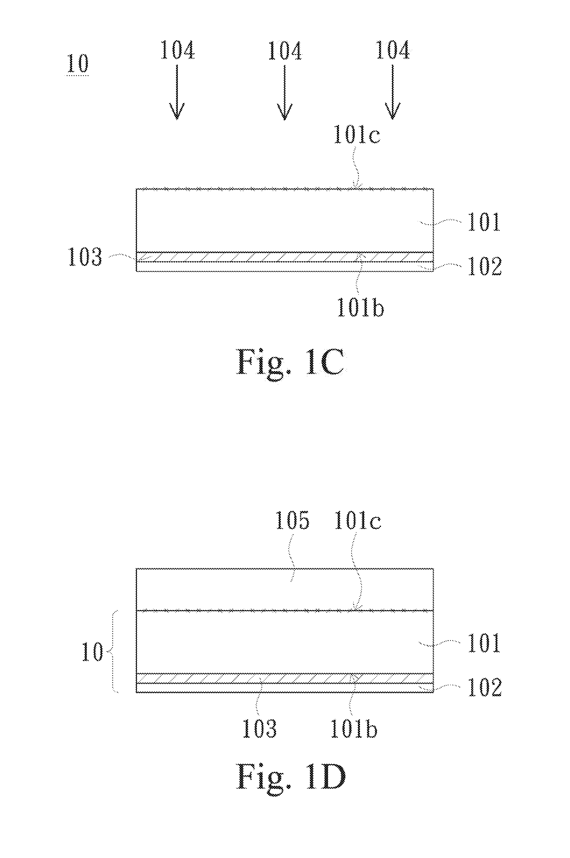
[0033]The present disclosure provides a metal substrate of double-sided substrate structure including two metal substrates of single-sided substrate structure bonded to each other through a release layer, and one of the insulating substrates of the metal substrates of the single-sided substrate structure can be temporarily bonded or debonded to the release layer (or called as insulating bonding layer), and thus to avoid fold damage, pad damage or delamin...


PUM

PropertyMeasurementUnit
glass transition temperatureaaaaaaaaaa
operating voltageaaaaaaaaaa
operating timeaaaaaaaaaa

Abstract

A metal substrate includes a first insulating substrate, a second insulating substrate, a first metal layer, a second metal layer and a release layer. The first insulating substrate has a first modified surface and a second surface opposite to the first modified surface. The first metal layer faces the second surface. The release layer is bonded on the first modified surface. The second insulating substrate is bonded on a side of the release layer, such that the release layer is between the first modified surface and the second insulating substrate. The second metal layer is disposed on a side of the second insulating substrate, such that the second insulating substrate is between the release layer and the second metal layer. An original surface roughness of the first modified surface has a variation substantially less than 10% after the first modified surface is released from the release layer.

Description

RELATED APPLICATIONS[0001]The present application is a Divisional Application of the U.S. application Ser. No. 14 / 476,752, filed Sep. 4, 2014, which claims priority to Taiwan Application Serial Number 103107985, filed Mar. 7, 2014, which is herein incorporated by reference.BACKGROUND[0002]1. Field of Invention[0003]The present disclosure relates to an electronic circuit substrate and a method of manufacturing the electronic circuit substrate. More particularly, the present disclosure relates to a metal substrate and a method of manufacturing the metal substrate.[0004]2. Description of Related Art[0005]A printed circuit board is an indispensable material in electronic products. A demand of the printed circuit board is increased with a growing demand of consumer electronic products. With the development toward compact size and flexibility for the electronic products, a flexible printed circuit hoard is widely applied recently in computers and its peripheral equipment, communication pr...

Claims


Application Information

Patent Timeline
Patent Type & Authority Applications(United States)
IPC IPC(8): H05K3/00H05K1/05H05K1/03
CPCH05K3/007H05K1/056H05K1/0313H05K1/0346H05K1/0393H05K3/0097H05K3/06H05K2201/0154H05K2201/0355H05K2203/1536Y10T428/1438Y10T428/24355Y10T156/10H05K2201/0133H05K2203/06H05K1/02H05K1/03H05K3/22H05K3/46B32B38/0008B32B37/12B32B2310/14H05K1/028H05K1/0298H05K3/0011H05K3/44H05K2203/10
Inventor LEE, HUNG-JUNG
Owner AZOTEK
Why Eureka
Try Eureka