Method for avoiding pixel saturation
- Summary
- Abstract
- Description
- Claims
- Application Information
AI Technical Summary
Benefits of technology
Problems solved by technology
Method used
Image

Examples
first embodiment
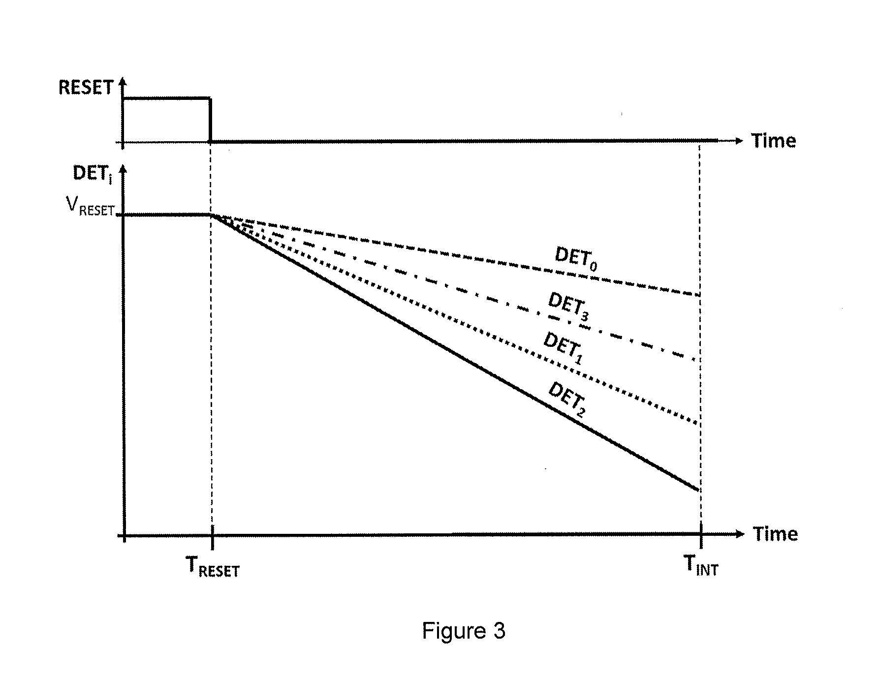
[0049]FIG. 6 illustrates the present invention with a synchronous reset pixel dealing with 4 pixels having each at least one detector node. It is made of 4 CMOS 3-T APS 7, 8, 9, 10, a lowest voltage detector block 11 having 4inputs, a comparator 12 and 1 extra transistor 13 added to each 3-T APS (so in total 4 extra transistors). The photodiodes of the 3-T APS do not necessarily have to be identical. The lowest voltage detector 11 inputs sense the detector nodes of the 4 APS: DET0, DET1, DET2, and DET3. Here, the comparator 12 can be made by either a comparator comparing DETX with a reference voltage VREF or a Schmitt trigger having its lower detection threshold equal to VREF, or any kind of circuitry capable of generating a pulsed signal from the output of the lowest voltage detector block, such as a monostable. The reset functionality of transistors 13 can be achieved by a dedicated logic circuitry and the re-use of the RESET transistors of the 3T APS.
[0050]FIG. 7 depicts the timi...
second embodiment
FIG. 8 illustrates the present invention, a block diagram of the synchronous reset pixel but with the addition of an ENCOMP pin 14 connected to the comparator 12. This ENCOMP pin 14 is added to define a shorter integration time (TINT-TEN). Indeed, detectors which have crossed the reference signal before ENCOMP pulse will restart their integration cycle but with a shorter time so that saturation until the end of exposure time TINT is impossible for these pixels. TEN is programmable and must be set to avoid pixel saturation. High level of the ENCOMP signal can be rather short and should be long enough to completely reset the pixels. FIG. 9 displays the timing diagram of the synchronous reset pixel as shown in FIG. 8, including lowest voltage detector 11 and comparator 12 plus its ENCOMP pin 14. Comparator 12 can only toggle its output if ENCOMP signal is set high. When ENCOMP signal is low, the pixels can saturate as if there would be no extra circuitry.
On top of that, a SRST_CNT sign...
third embodiment
[0051]A third embodiment is presented FIG. 11. FIG. 11 shows a block diagram of the synchronous reset pixel but with the addition of an ENCOMP pin 14 connected to both the lowest voltage detector 11 and the comparator 12.
[0052]FIG. 12 shows the same input conditions than FIG. 9. The only change resides in the ENCOMP pin 14, connected to both lowest voltage detector 11 and comparator 12. DETX copies the lowest voltage among DET0, DET1, DET2, and DET3 only when ENCOMP signal is high. The outcome for SRST and SRST_CNT signals is identical for both configurations.
[0053]Those second and third embodiments have the benefit of saving current as lowest voltage detection and comparison are only made when ENCOMP signal is set high. Indeed, the comparator 12 works as an analog “voltage comparator”, and its current consumption will be linked to its input voltage. With the addition of the ENCOMP pin 14, the comparator 12 and occasionally the lowest voltage detector 11 will only consume current a ...
PUM
 Abstract
Description
Claims
Application Information
 - R&D Engineer
- R&D Manager
- IP Professional
- Industry Leading Data Capabilities
- Powerful AI technology
- Patent DNA Extraction
Browse by: Latest US Patents, China's latest patents, Technical Efficacy Thesaurus, Application Domain, Technology Topic.
© 2024 PatSnap. All rights reserved.Legal|Privacy policy|Modern Slavery Act Transparency Statement|Sitemap