Gate driving circuit and display device

a driving circuit and display device technology, applied in the direction of generating/distributing signals, digital storage, instruments, etc., can solve the problems of poor driving efficiency, degradation of display quality, and too much power consumption, so as to reduce delay and power consumption, improve driving efficiency, and reduce rc loading

Active Publication Date: 2016-11-17
HANNSTAR DISPLAY NANJING +1
View PDF7 Cites 12 Cited by
  • Summary
  • Abstract
  • Description
  • Claims
  • Application Information

AI Technical Summary

Benefits of technology

[0006]An objective of the present invention is to provide a gate driving circuit and a display device for reducing RC loading, thereby improving driving efficiency and reducing delay and power consumption.

Problems solved by technology

However, for a high definition (HD) display device or an ultra HD display device, the gate driver is in charge of driving more pixels, resulting in over resistance-capacitance (RC) loading of the clock signal lines of the gate driver, thus causing too much power consumption and poor driving efficiency, leading to degradation of display quality.

Method used


Image

  • Gate driving circuit and display device
  • Gate driving circuit and display device
  • Gate driving circuit and display device

Examples


first embodiment

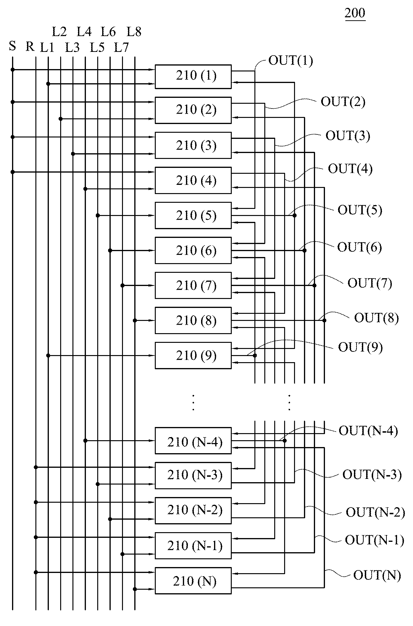
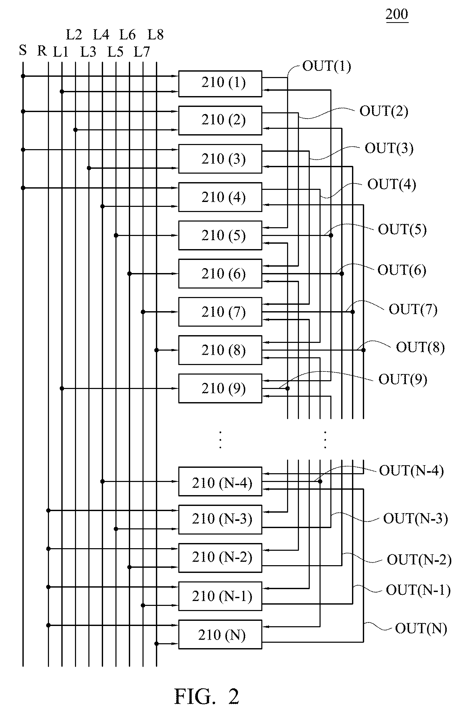
[0033]Please refer to FIG. 2, which is a schematic diagram of a gate driving circuit 200 in accordance with the present invention. The gate driving circuit 200 is adapted to the display device 100 of FIG. 1 or other similar display device. In the following, the display device 100 of FIG. 1 is exemplified for description. The gate driving circuit 200 is a part of the gate driver 130. The gate driving circuit 200 includes clock signal lines L1-L8, a starting signal line S, an ending signal line R and N stage shift registers 210(1)-210(N), where N is an integer greater than or equal to 9. In some embodiments, N is a multiple of 8. The clock signal lines L1-L8 are configured to provide clock signals C1-C8 to the corresponding shift registers 210(1)-210(N). In FIG. 2, the clock signal lines L1-L8 respectively provide the clock signals C1-C8 to the corresponding shift registers 210(1)-210(N). In addition, the starting signal line S provides a starting signal STV to the 1st to 4th stage sh...

second embodiment

[0036]The concept of the aforementioned embodiments may also be applied to a display device which is driven simultaneously at left and right sides. Please refer to FIG. 4, which is a schematic diagram of the gate driving circuit 400 in accordance with the present invention. The gate driving circuit 400 is adapted to the display device 100 of FIG. 1 or another similar display device. In the following, the display device 100 of FIG. 1 is exemplified for description.

[0037]The gate driving circuit 400 is a part of the gate driver 130, and is divided into a first gate driving circuit 400A and a second gate driving circuit 400B. The first gate driving circuit 400A includes clock signal lines L1-L8, a starting signal line S, an ending signal line R and first N stage shift registers 410A(1)-410A(N), and the second gate driving circuit 400B includes clock signal lines LV-L8′, a starting signal line S′, an ending signal line R′ and second N stage shift registers 410B(1)-410B(N), where N is an...

third embodiment

[0041]Please refer to FIG. 6, which is a structure diagram of a driving circuit 600 in accordance with the present invention. The driving circuit 600 is adapted to the display device 500 of FIG. 5 or other similar display device. In the following, the display device 500 of FIG. 5 is exemplified for description. The driving circuit 600 includes gate driving circuits 600A and 600B which are respectively a part of the gate drivers 530A and 530B. The gate driving circuit 600A includes clock signal lines L1, L3, L5, L7, L9, L11, L13 and L15, a start signal line S1, an ending signal line R1 and odd-numbered stage shift registers 610(1), 610(3), . . . , 610(N−1), and the gate driving circuit 600B includes clock signal lines L2, L4, L6, L8, L10, L12, L14 and L16, a starting signal line S2, an ending signal line R2 and even-numbered stage shift registers 610(2), 610(4), . . . , 610(N), where N is an integer greater than or equal to 17. In some embodiments, N is a multiple of 16. The clock si...


PUM


Abstract

The invention discloses a gate driving circuit and a display device. The gate driving circuit includes first to eighth dock signal lines and first to Nth stage first shift registers, where N is an integer greater than or equal to 9. The first to eighth clock signal lines are configured to provide first to eighth clock signals, respectively. The ith stage first shift register is coupled to one of the first to eighth clock signal lines and receives one of the first to eighth clock signals, a first input signal and a second input signal and outputs an ith stage first output signal, where i is any integer from 1 to N.

Description

RELATED APPLICATIONS[0001]This application claims priority to Chinese Patent Application Serial Number 201510242906.9, filed on May 13, 2015, which is herein incorporated by reference.BACKGROUND[0002]1. Field of the Invention[0003]The present invention relates to a gate driving circuit and a display device, and more particularly to a gate driving circuit and a display device which can improve driving efficiency and reduce power consumption.[0004]2. Description of Related Art[0005]A flat panel display device, such as a liquid crystal display (LCD) device or an organic light-emitting diode (OLED) display device, generally has a lot of shift registers for controlling gray levels of all pixels displayed in the display device at the same time point. However, for a high definition (HD) display device or an ultra HD display device, the gate driver is in charge of driving more pixels, resulting in over resistance-capacitance (RC) loading of the clock signal lines of the gate driver, thus ca...

Claims


Application Information

Patent Timeline
Patent Type & Authority Applications(United States)
IPC IPC(8): G09G3/20G06F1/04G09G5/14G11C19/00
CPCG09G3/2085G11C19/00G09G3/2092G06F1/04G09G2330/021G09G2310/08G09G2310/0286G09G2310/0243G09G2310/0283G09G5/14G11C19/28G09G3/20G09G3/3266G09G3/3677G09G2310/0213
Inventor LIN, SUNG-CHUNLIU, HSUAN-CHENCHAN, CHIEN-TING
Owner HANNSTAR DISPLAY NANJING
Why Eureka
Try Eureka