Light-receiving device and manufacturing method thereof

a technology of light-emitting devices and manufacturing methods, which is applied in the direction of radiation-controlled devices, semiconductor devices, electrical apparatus, etc., can solve the problems of limiting the actual aperture ratio, low light utilization rate, and large loss of incident light, so as to reduce the risk of deterioration of the properties of the photodiode or damage of the photodiode at the time of providing the wiring

Inactive Publication Date: 2016-11-17
PANASONIC INTELLECTUAL PROPERTY MANAGEMENT CO LTD
View PDF7 Cites 0 Cited by
  • Summary
  • Abstract
  • Description
  • Claims
  • Application Information

AI Technical Summary

Benefits of technology

[0037]In addition, since a wiring is not directly provided on the transparent conductive film on the photodiode, a risk of deterioration of properties of the photodiode or a damage of the photodiode due to stress at the time of providing the wiring can be reduced.
[0038]Also, since a voltage is supplied to the transparent conductive film using a rewiring of a thick film having low resistance, supplying of the voltage can be stabilized.

Problems solved by technology

In the light-receiving device having such a structure, since the photodiode and the scanning element are disposed on the same plan surface, an aperture ratio (ratio of amount of light incident on photoelectric converter with respect to amount of light incident on light receiving surface) is low and a light utilization rate is low, and thus a loss of incident light is great.
An actual aperture ratio is improved when on-chip microlenses are developed, and the like; however, there is a limit that the actual aperture ratio is improved, as long as the photodiode and the scanning element are disposed on the same plan surface.
Therefore, for example, unlike a case of a photoconductive type image pick-up tube of which a photoconductive film is formed on a smooth glass substrate, there is a problem in that dark current is increased by a local electric field concentration caused by the unevenness of a base and a defect of white dots on a screen is likely to be generated.
Particularly, in a case in which high sensitivity is obtained using the avalanche multiplication phenomenon in the photodiode, it is necessary that a strong electric field is applied to the photodiode, and thus injecting of a local dark current or an avalanche breakdown due to non-uniformity of the electric field is likely to be generated.

Method used


Image

  • Light-receiving device and manufacturing method thereof
  • Light-receiving device and manufacturing method thereof
  • Light-receiving device and manufacturing method thereof

Examples


first exemplary embodiment

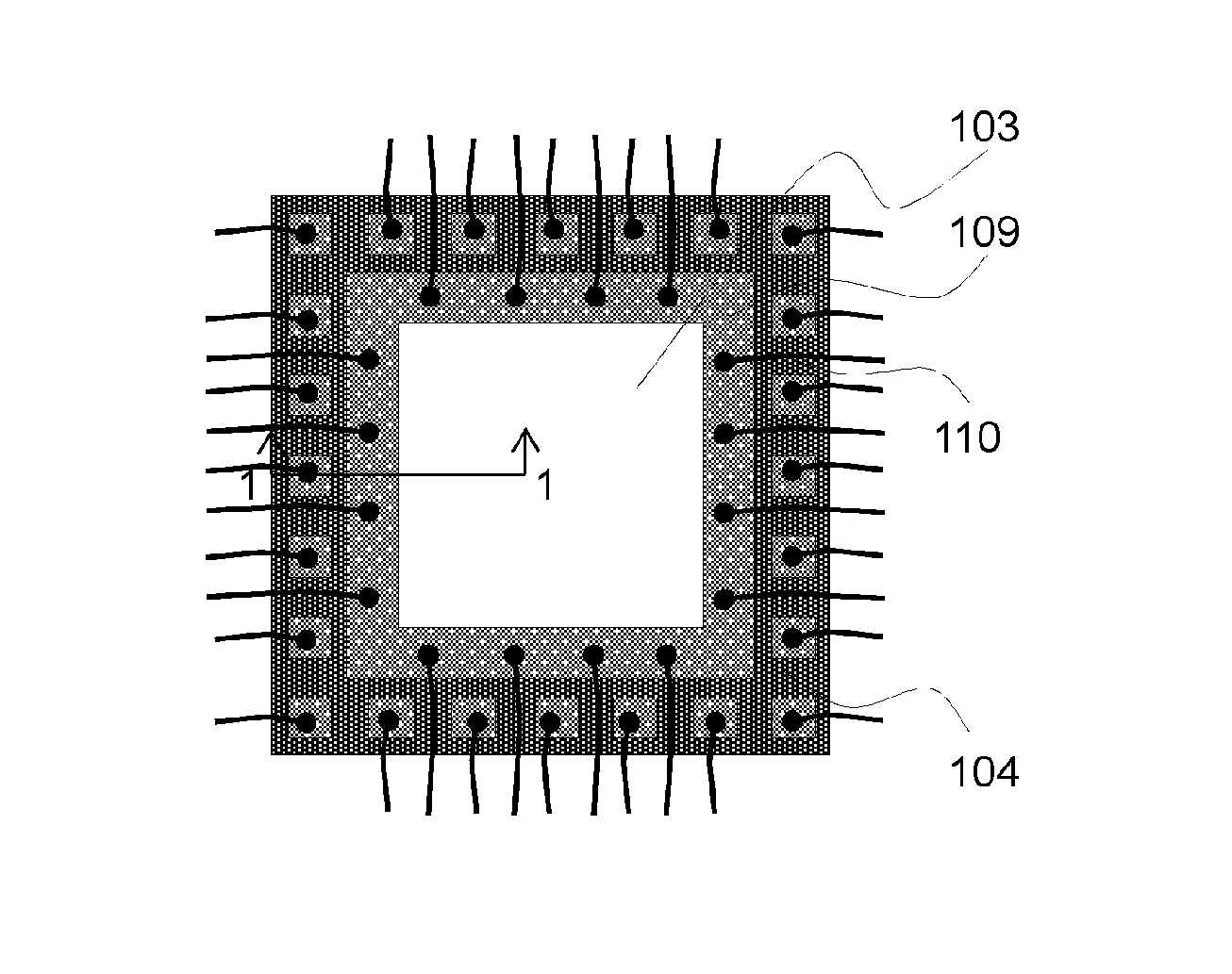
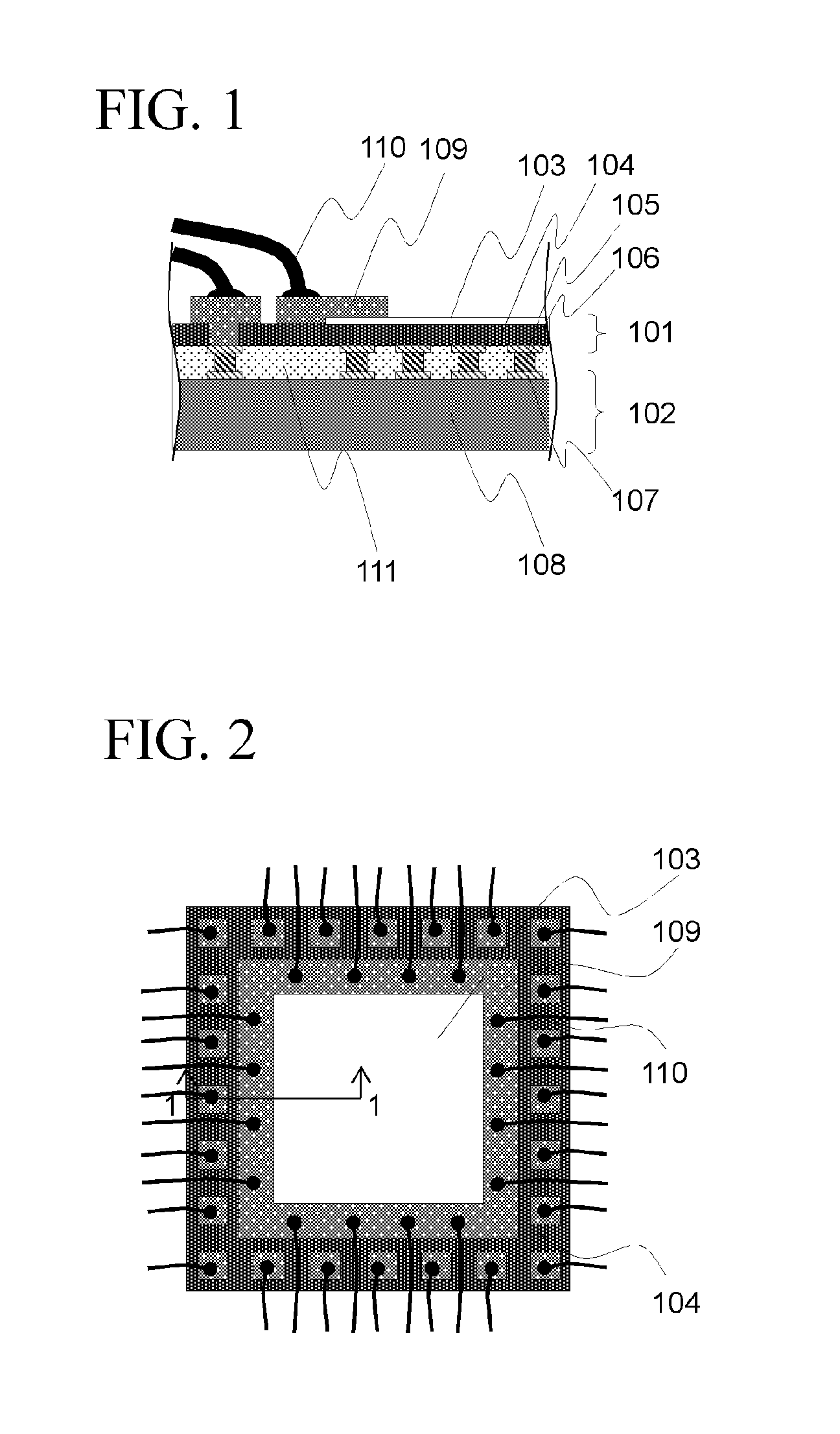
[0064]FIG. 1 is a sectional view of a light-receiving device according to a first exemplary embodiment of the disclosure. The light-receiving device is a laminate type device structure in which first pixel electrode 105 formed on photoelectric converter 101 and second pixel electrode 107 formed on scanning circuit unit 102 are connected to each other by microbump 106. Transparent conductive film 103 is formed on photodiode 104 of photoelectric converter 101. Rewiring 109 for supplying power to scanning circuit unit 102 and a photodiode is formed on transparent conductive film 103, and rewiring 109 is electrically connected to an external electrode by wire 110.

[0065]Peripheries of microbump 106 are covered with protection film 111, and rewiring 109 is formed directly on at least one of first pixel electrodes 105.

[0066]FIG. 2 is a top view of the light-receiving device according to the disclosure. A part of an upper surface of transparent conductive film 103 is covered with rewiring 1...

second exemplary embodiment

[0087]FIG. 4 is a sectional view of a light-receiving device according to a second exemplary embodiment of the disclosure, and FIG. 5 is a plan view.

[0088]Referring to FIG. 4 and FIG. 5, peripheries of photodiode 104 are covered with resin 114.

[0089]Rewiring 109 is formed on resin 114 and photodiode 104, and is electrically connected to an external electrode by wire 110.

[0090]As seen from the above, since the peripheries of photoelectric converter 101 are covered with resin 114 and a size of a plan of photoelectric converter 101 itself can be reduced, the number of devices mounted near the wafer is increased, and costs of the devices can be reduced.

[0091]Further, a restriction in which photoelectric converter 101 and scanning circuit unit 102 are made the same size can be released, and a degree of freedom in design of the device is significantly improved.

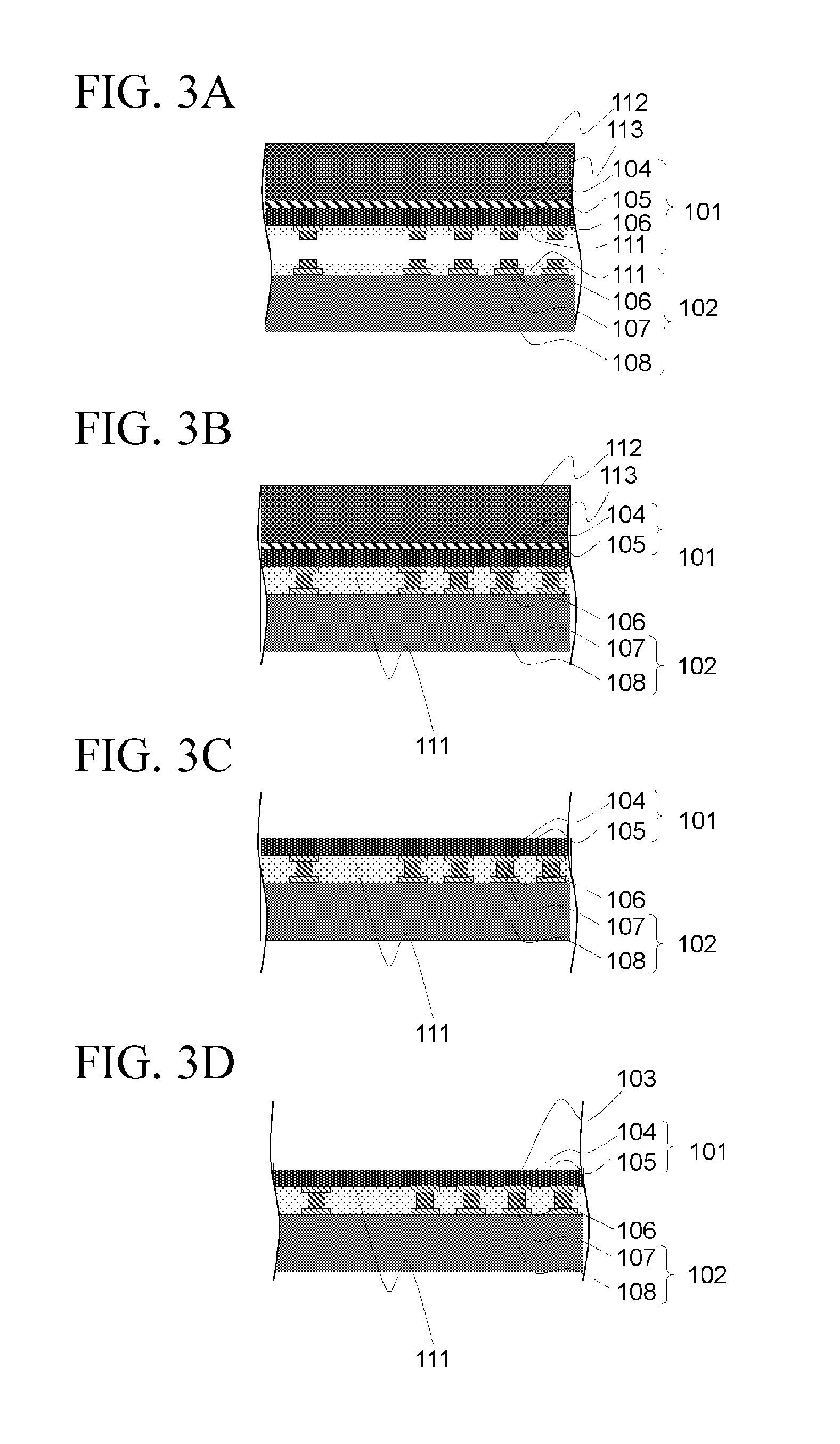
[0092]FIG. 6A to FIG. 6I are sectional views relating to a manufacturing method of the light-receiving device according to the sec...

third exemplary embodiment

[0103]FIG. 7 is a sectional view of a light-receiving device according to a third exemplary embodiment of the disclosure, and FIG. 8 is a plan view thereof.

[0104]Referring to FIG. 7 and FIG. 8, rewiring 109 can be formed in a grid shape between pixel electrodes on an upper surface of transparent conductive film 103 of photodiode 104, so that the OB region is removed and incident light into pixel electrodes is not inhibited.

[0105]As described above, rewiring 109 on transparent conductive film 103 between pixel electrodes where the OB region is removed is wound in a grid shape, thereby making it possible to reduce dispersion of voltage applying due to a positional relationship of rewiring 109 and photodiode 104.

[0106]The disclosure is not limited to the exemplary embodiments described above, and there is a variety of other forms changed within a range in consideration of those skilled in the art with respect to the exemplary embodiments, and the like, without departing from the spirit...


PUM


Abstract

A light-receiving device which has high reliability and high sensitivity is provided with low cost. The device has a laminate type device structure in which a photoelectric converter and a scanning circuit unit are connected by microbumps, and a structure in which a transparent conductive film is formed on a photodiode of a photoelectric converter. A rewiring is formed so as to have a function of an OB region, and an electrode for supplying a voltage to a scanning circuit and the photodiode on the transparent conductive film, and the rewiring is electrically connected to an external electrode by a wire.

Description

BACKGROUND[0001]1. Technical Field[0002]The present disclosure relates to a light-receiving device which converts incident light into an electric signal, particularly, to a light-receiving device in which semiconductor scanning circuits, which read a signal of electrical charge converted from incident light using a photodiode having a photoelectric conversion function, are laminated, and a manufacturing method thereof.[0003]2. Description of the Related Art[0004]As a light-receiving device of the related art, a light-receiving device in which a photodiode of a photoelectric converter and a scanning element transmitting photocharge generated by the photodiode are integrated on a semiconductor substrate, is developed and is commercially used.[0005]In the light-receiving device having such a structure, since the photodiode and the scanning element are disposed on the same plan surface, an aperture ratio (ratio of amount of light incident on photoelectric converter with respect to amoun...

Claims


Application Information

Patent Timeline
Patent Type & Authority Applications(United States)
IPC IPC(8): H01L27/146
CPCH01L27/14634H01L27/14623H01L27/14636H01L27/1469H01L2224/48463
Inventor DOHI, SHIGEFUMI
Owner PANASONIC INTELLECTUAL PROPERTY MANAGEMENT CO LTD
Why Eureka
Try Eureka