Touch-sensing quantum dot LCD panel

a quantum dot and touch sensing technology, applied in the direction of instruments, planar/plate-like light guides, mechanical instruments, etc., can solve the problems of reducing the optical quality of the display device, adding an undesired thickness and complexity to the display device, and reducing the transmission light sensed

Inactive Publication Date: 2016-11-24
FLATFROG LAB
View PDF12 Cites 91 Cited by
  • Summary
  • Abstract
  • Description
  • Claims
  • Application Information

AI Technical Summary

Benefits of technology

[0008]It is an object of the invention to at least partly overcome one or more of the above-identified limitations of the prior art. More specifically, it is an object of the invention to provide a solution for optical touch-sensing display panels, which limits the demand placed on the system in relation to light emitters. Another object is to reduce the required thickness for providing touch sensitivity to a display device.

Problems solved by technology

The major drawback of these techniques is that they reduce the optical quality of the display device, by reducing the amount of light emitted from the display or by reducing the number of active pixels of the display device.
The light may be disturbed (frustrated) by an object touching the light guide, whereby a decrease in transmitted light is sensed at certain light detection points.
Providing a display device with this touch sensing system would add an undesired thickness and complexity to the display device.
A challenge connected to the art of optical touch-sensing systems is the provision of light emitters and detectors, and to the coupling of light in and out of the light guide.

Method used


Image

  • Touch-sensing quantum dot LCD panel
  • Touch-sensing quantum dot LCD panel
  • Touch-sensing quantum dot LCD panel

Examples


Embodiment Construction

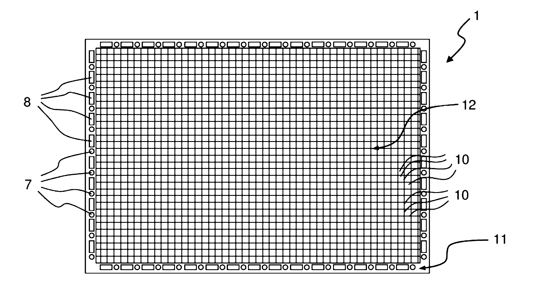
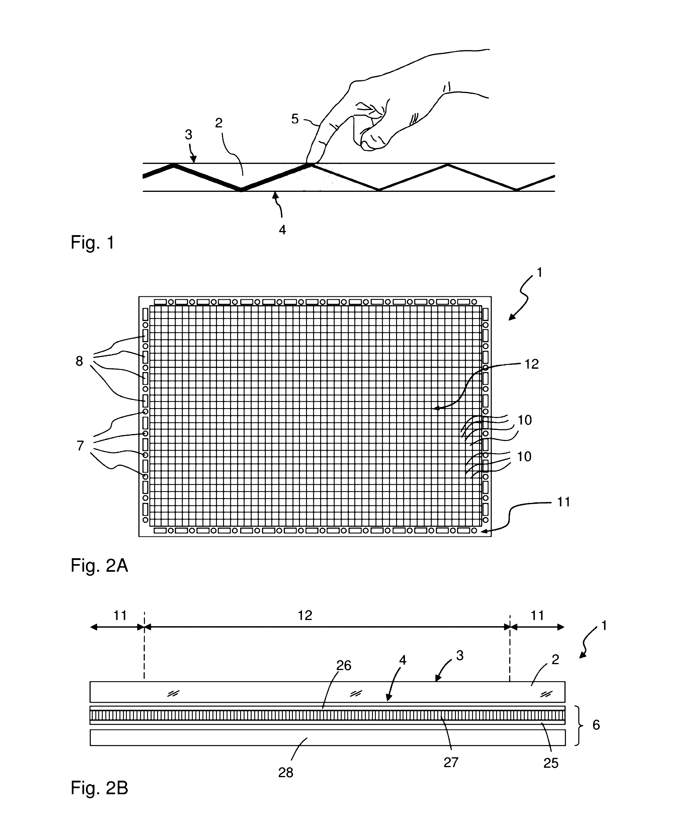
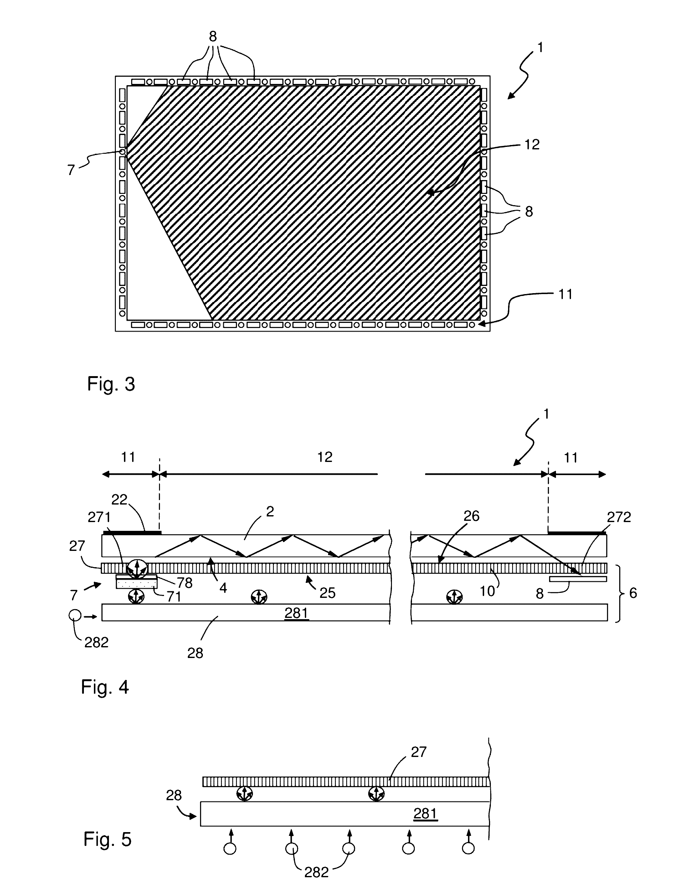
[0047]The present invention relates to the use of optical techniques, specifically FTIR, for providing touch sensitivity to a display apparatus. More specifically, the invention provides a truly integrated touch-sensing display panel 1, operating by means of FTIR in a liquid crystal display (LCD) device. Throughout the description the same reference numerals are used to identify corresponding elements.

[0048]FIG. 1 illustrates the operating principle of a touch-sensing FTIR system. In the side view of FIG. 1, a beam of light is propagated by total internal reflection (TIR) inside a planar (two-dimensional) light guide 2. The light guide 2 comprises opposing surfaces 3, 4 which define a respective boundary surface of the light guide 2. Each boundary surface 3, 4 reflects light that impinges on the boundary surface from within the light guide 2 at an angle that exceeds the so-called critical angle, as is well-known to the skilled person. When an object 5 is brought sufficiently close t...


PUM

PropertyMeasurementUnit
diameteraaaaaaaaaa
diameteraaaaaaaaaa
particle sizeaaaaaaaaaa

Abstract

A touch-sensing display panel comprising: an LCD unit including a backlight unit and a plurality of image-forming pixel elements arranged in a central region; a light emitter emulated by passing light through a pixel element of a first selected portion of a peripheral region of the LCD unit, said emitter including a first quantum dot structure connected to receive excitation light from said backlight unit so as to emit light at longer wavelength than said excitation light; a planar light guide having a front surface forming a touch-sensing region and an opposite rear surface facing the LCD unit, said light guide being connected to receive emitter light for propagation therein through total internal reflection; a light detector connected to receive light from the light guide.

Description

CROSS-REFERENCE TO RELATED APPLICATIONS[0001]This application claims the benefit and priority to and is a U.S. National Phase of PCT International Application Number PCT / SE2015 / 050041, filed on Jan. 16, 2015. This application claims the benefit and priority to Swedish patent application No. 1450037-5, filed 16 Jan. 2014. The disclosure of the above-referenced applications are hereby expressly incorporated by reference in their entirety.TECHNICAL FIELD[0002]The present invention relates to touch sensing systems implemented with a display, and especially to liquid crystal display devices that employ quantum dot technology and offer optical touch sensitivity.BACKGROUND ART[0003]Display devices with touch sensitivity are used today in a wide variety of applications such as touch pads in laptop computers, all-in-one computers, mobile phones and other hand-held devices, etc. It is often a desire to provide these electronic devices with a relatively large touch sensing display and still le...

Claims


Application Information

Patent Timeline
Patent Type & Authority Applications(United States)
IPC IPC(8): G06F3/042F21V8/00G02F1/1335G02F1/1368G06F3/041G02F1/1333
CPCG06F3/0421G06F3/0412G02F1/13338G02F1/133621G02F2001/133614G02B6/005G02F1/133603G06F2203/04109G02F2202/36G02F1/1368G06F3/0428G02F1/133614
Inventor WASSVIK, OLA
Owner FLATFROG LAB
Why Eureka
Try Eureka