
Raman microscopic imaging device

a technology of imaging device and microscopy, which is applied in the direction of optical radiation measurement, instruments, spectrometry/spectrophotometry/monochromators, etc., can solve the problems of limited application capabilities, high cost of typical srs image-producing device, and high method sensitiveness, so as to avoid light loss, outstanding beam quality, and high stability over time

Active Publication Date: 2016-12-15
LEICA MICROSYSTEMS CMS GMBH
View PDF6 Cites 3 Cited by
  • Summary
  • Abstract
  • Description
  • Claims
  • Application Information

AI Technical Summary

Benefits of technology

The invention describes an affordable and reliable Raman microscopy imaging device that uses a small number of optical elements and avoids light losses. By using a continuously operating laser light source, the device eliminates the need for a delay stage and avoids intensity peaks in the measured signal. Additionally, the device can use a femtosecond laser or picosecond laser as a pulsed source for use in a CRSM method. These technical effects make the device more efficient and reliable for imaging applications.

Problems solved by technology

Because of the modulation and demodulation techniques explained above that are utilized in the SRS method, however, this method is also very sensitive in terms of the delay that must be established between the laser beams emitted from the two pulsed laser light source, in terms of the pulse synchronization that must exist during operation of the two pulsed laser light sources, and in terms of the time-related cyclical “jitter” that often occurs when the pulsed laser light sources are operated.
A typical SRS image-producing device is moreover comparatively costly, and is limited with regard to its application capabilities.
It is evident from this that a device operating according to the SRS method with two continuous laser light sources is unsuitable for real-time image generation, in which approximately 25 individual images must be generated every second.
In addition, continuous laser light sources adjustable over a broad wavelength band are in any case not yet readily available at this time.

Method used


Image

  • Raman microscopic imaging device
  • Raman microscopic imaging device
  • Raman microscopic imaging device

Examples


Embodiment Construction

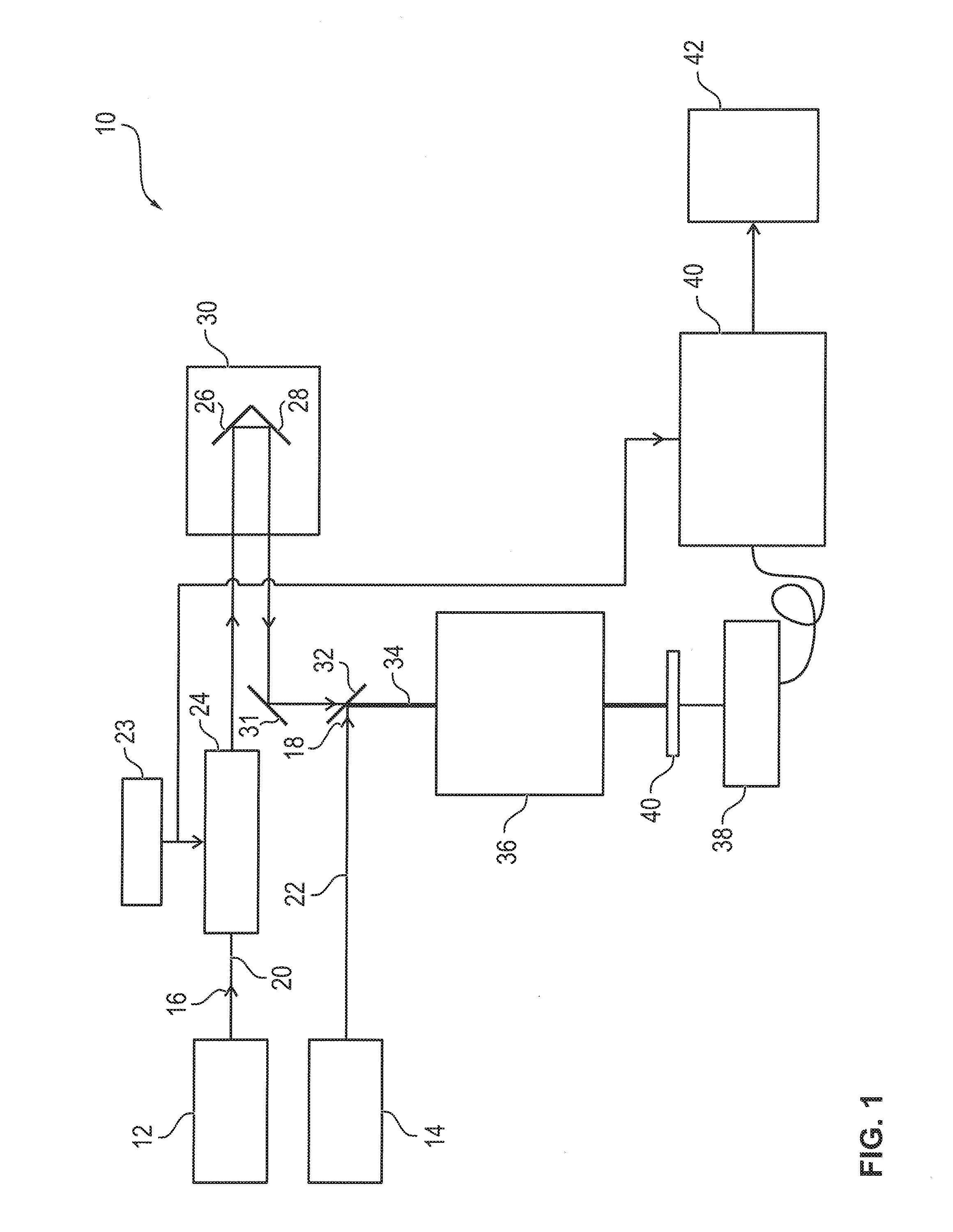
[0035]Firstly an SRS imaging device not covered by the invention will be described as a comparative example with reference to FIGS. 1 and 2, and then the approach according to the present invention will be explained on the basis of that comparative example.

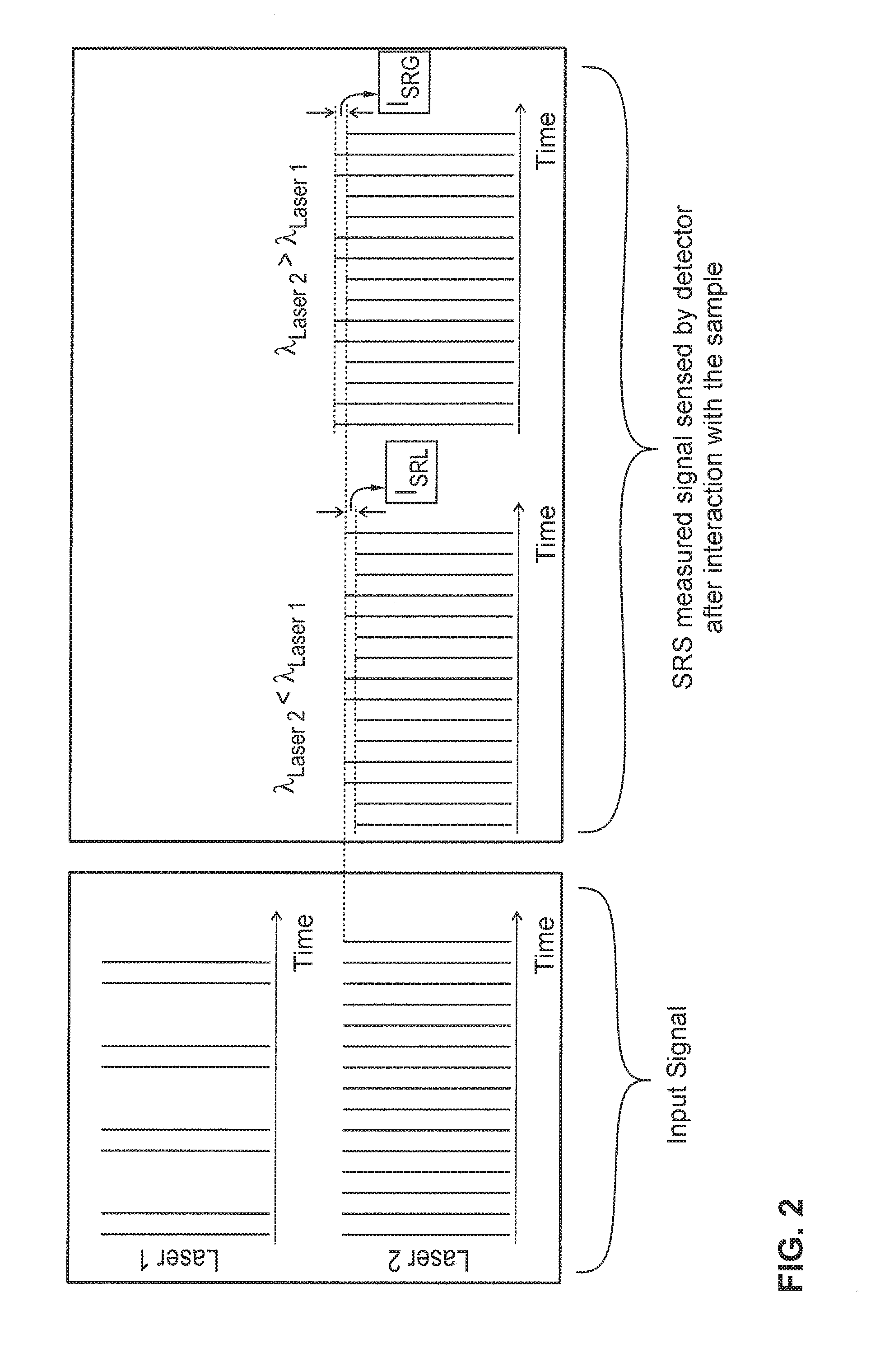
[0036]The SRS imaging device designated in general as 10 in FIG. 1 contains a first pulsed laser light source 12 and a second pulsed laser light source 14. The two pulsed laser light sources 12 and 14 emit pulsed laser beams 16 and 18 respectively along a first light path 20 and a second light path 22. One of these laser beams 16, 18 functions in SRS imaging as a pump beam, and the other laser beam as a Stokes beam. The laser beam that has the lesser wavelength is typically referred to as a “pump beam,” while the laser beam having the greater wavelength is referred to as a “Stokes beam.”

[0037]In the arrangement according to FIG. 1, first laser beam 16 emitted along first light path 20 from pulsed laser light source 12 is amplitude...


PUM


Abstract

A Raman microscopy imaging device (100) is described, having: a first laser light source (12) for emitting a first laser beam (16) having a first wavelength along a first light path (20); a second laser light source (44) for emitting a second laser beam (18) having a second wavelength, different from the first wavelength, along a second light path (22) physically separated from the first light path (20); a beam combining element (32) for collinearly combining the two laser beams (16, 18) in one shared light path (34) directed onto a sample; a detector (38) for sensing a measured signal on the basis of the two laser beams (16, 18) interacting with the sample; and an evaluation unit (40) for evaluating the measured signal sensed by the detector (38). According to the present invention the first laser light source (12) is embodied as a pulsed source, and the second laser light source (44) as a continuous source.

Description

CROSS-REFERENCE TO RELATED APPLICATIONS[0001]The present application is the U.S. national phase of International Application No. PCT / EP2014 / 075049 filed Nov. 19, 2014, which claims priority of German Application No. 10 2013 112 759.2 filed Nov. 19, 2013, the entirety of which is incorporated herein by reference.FIELD OF THE INVENTION[0002]The invention relates to a Raman microscopy imaging device, having a first laser light source for emitting a first laser beam having a first wavelength along a first light path; a second laser light source for emitting a second laser beam having a second wavelength, different from the first wavelength, along a second light path physically separated from the first light path; a beam combining element for collinearly combining the two laser beams in one shared light path directed onto a sample; a detector for sensing a measured signal on the basis of the two laser beams interacting with the sample; and an evaluation unit for evaluating the measured s...

Claims


Application Information

Patent Timeline
IPC IPC(8): G01N21/65G01J3/10G01J3/44
CPCG01N21/65G01N2021/655G01J3/10G01J3/44G01J3/0227
Inventor KRISHNAMACHARI, VISHNU VARDHANSEYFRIED, VOLKERHAY, WILLIAM C.
Owner LEICA MICROSYSTEMS CMS GMBH
Learn More