

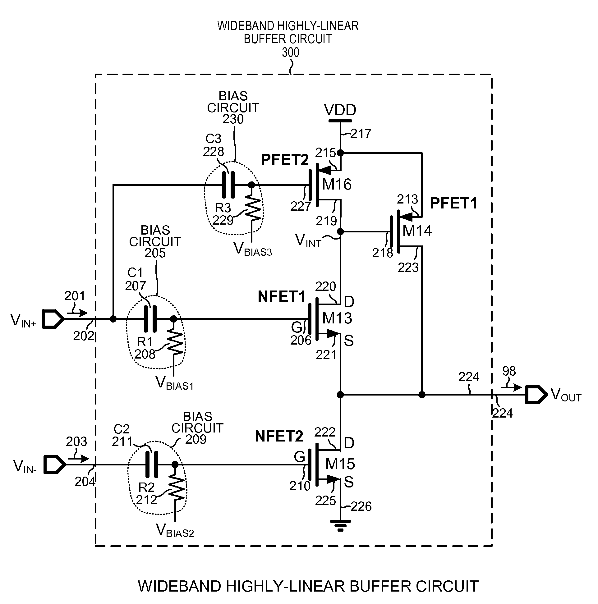
Wideband Highly-Linear Low Output Impedance D2S Buffer Circuit
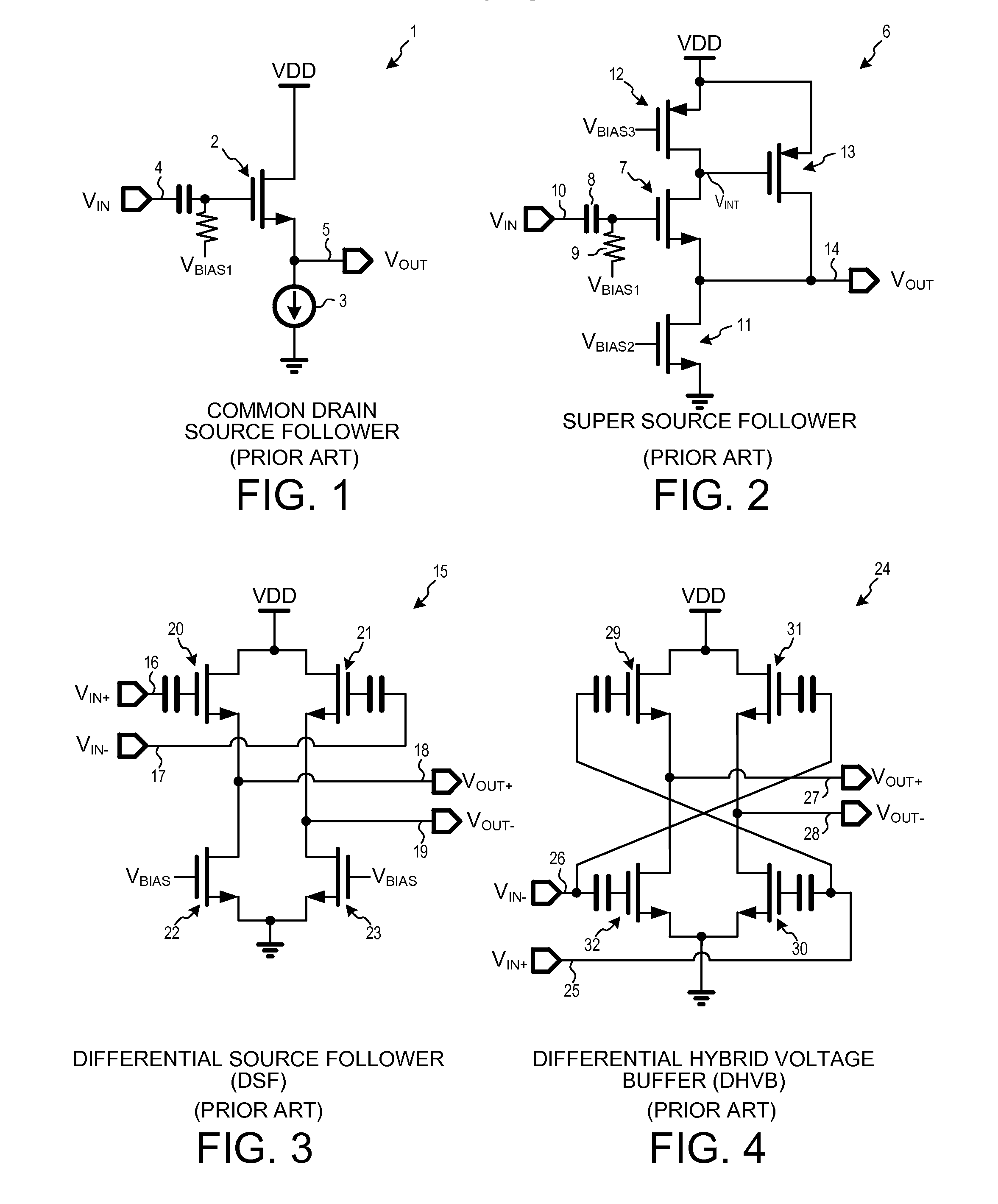
a buffer circuit and high output impedance technology, applied in logic circuit coupling/interface arrangement, logic circuit coupling/interface using field-effect transistors, pulse techniques, etc., can solve the problem that the circuit of fig. 3 is not really suitable for driving a single-ended signal, and the output impedance of the second stage is not sufficiently low to drive the low impedance load with adequate linearity, etc. problem, to achieve the effect of low output impedance, low power consumption and high output impedance problem
- Summary
- Abstract
- Description
- Claims
- Application Information
AI Technical Summary
Benefits of technology
Problems solved by technology
Method used
Image

Examples
Embodiment Construction
[0034]Reference will now be made in detail to background examples and some embodiments of the invention, examples of which are illustrated in the accompanying drawings.
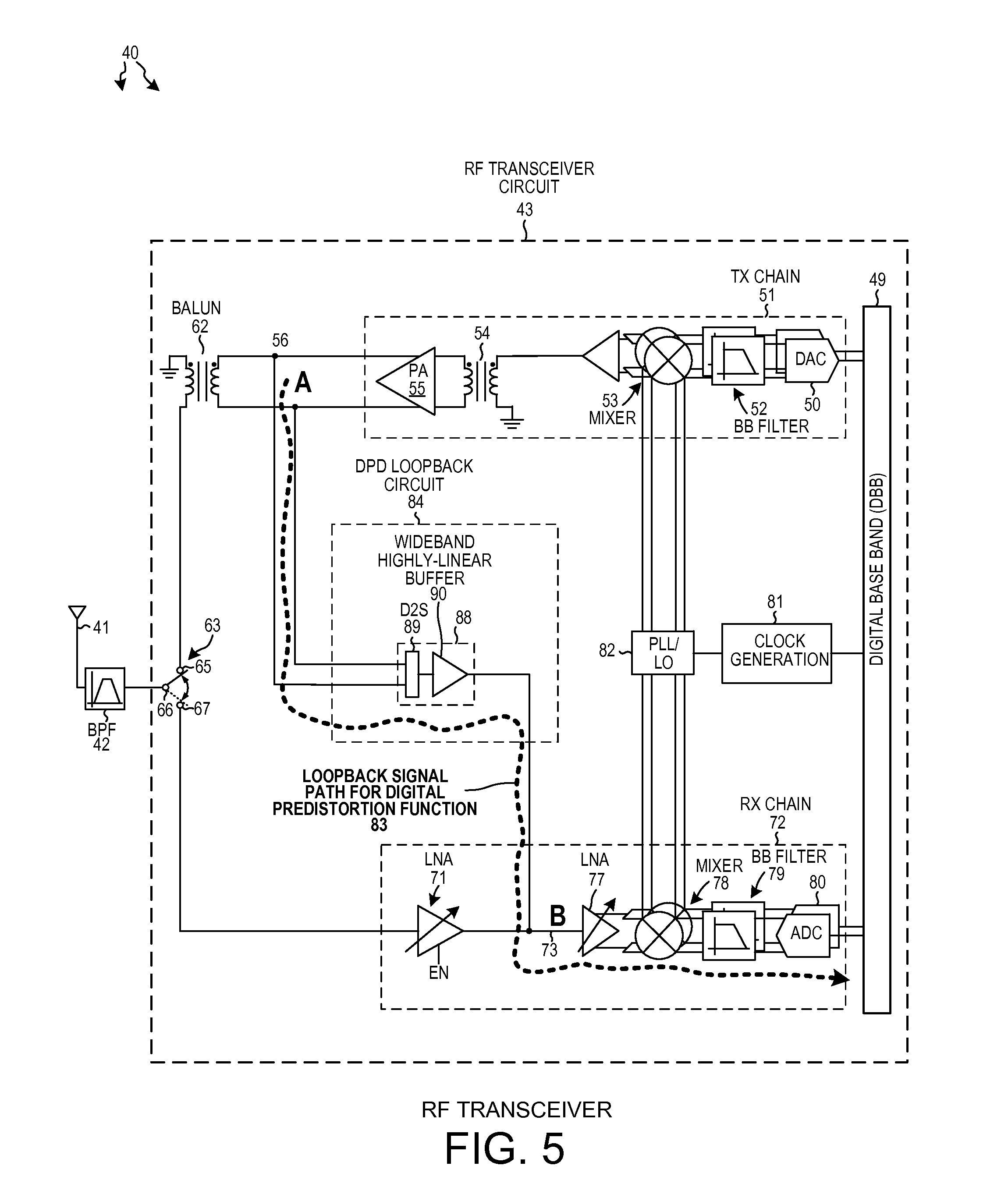
[0035]FIG. 5 is a circuit diagram of a Radio Frequency (RF) transceiver 40 in accordance with one novel aspect. The RF transceiver 40 includes an antenna 41, a band pass filter 42 (optional), and an RF transceiver circuit 43. The transceiver integrated circuit 44 includes a Digital Baseband (DBB) portion 49. When the RF transceiver 40 is transmitting, a stream of digital values output by the DBB portion 49 is supplied to a Digital-to-Analog Converter (DAC) 50 of a transmit chain 51. The transmit chain 51 includes the DAC 50, a Baseband (BB) filter 52, a mixer 53, a transformer 54, and a Power Amplifier (PA) 55. The DAC 50 converts the stream of digital values into a corresponding analog signal, and the analog signal is filtered by the BB filter 52, and is upconverted to an RF transmission frequency by mixer 53. The up...
PUM
 Abstract
Description
Claims
Application Information