Output buffer with inductive voltage divider

a voltage divider and output buffer technology, applied in the field of output buffers, can solve the problems of reducing limiting the precision of the oscillator output frequency, and limiting the performance of the oscillator circuit b>20/b>, so as to reduce the loading of the oscillator circuit, reduce phase noise, and increase the loading quality factor

Active Publication Date: 2006-03-09
INFINEON TECH AG
View PDF3 Cites 16 Cited by
  • Summary
  • Abstract
  • Description
  • Claims
  • Application Information

AI Technical Summary

Benefits of technology

[0015] According to another aspect of the present invention, the inductive voltage divider circuit comprises a first and second pair of series-connected inductances coupled to the differential output of the oscillator circuit. An output of the inductive voltage divider circuit comprises a pair of nodes between the series-connected inductances of each pair. Depending upon a relative magnitude of the series-connected inductances, an optimization can be made between a reduced loading on the oscillator circuit (e.g., increased loaded quality factor and thus reduced phase noise) and increased signal amplitude at the buffer input. In addition, a total inductance of the series-connected inductances is selected to optimize a maximum signal amplitude at the oscillator core output.
[0016] According to yet another aspect of the present invention, the series-connected inductances of the inductive voltage divider comprise differential longitudinally extending micro-strip lines having one or more shorting conductors extending therebetween. By a selective cutting or removal of one or more shorting conductors, a magnitude of the inductances may be altered, thereby facilitating a tuning of the oscillator loading / amplitude optimization.
[0017] In accordance with still another aspect of the present invention, the output buffer further comprises an emitter follower circuit coupled to the inductive voltage divider. The emitter follower circuit is configured to provide a decoupling function between the oscillator output and any succeeding stages of the buffer. It operates as an impedance transformation circuit, wherein its substantially high input impedance reduces the loading of the oscillator and its substantially low output impedance improves the driving condition for any succeeding stages and thus the speed of the oscillator system.
[0018] In still another aspect of the invention, a signal amplifying circuit is provided in the output buffer, for example, in the form of a differential transadmittance stage or an emitter-coupled pair circuit. Since a decoupling function of the emitter follower circuit is decreased at high oscillator frequencies, the emitter-coupled pair also serves to provide improved decoupling between the oscillator circuit and the load.
[0019] According to yet another aspect of the present invention, the output buffer circuit further comprises a differential base-grounded transistor circuit coupled to the emitter-coupled pair to form a cascode stage. The base-grounded transistor circuit provides further decoupling of the oscillator circuit from the load and also operates to reduce a time constant at the output of the emitter coupled pair circuit, thereby improving the speed of the oscillator system. Moreover, due to the comparatively high breakdown voltage of the base-grounded transistor circuit configuration, the output signal and, thus, the maximum output power provided by the buffer can be increased.
[0020] According to another aspect of the invention, the output buffer further comprises a bias current circuit coupled between the emitter coupled pair circuit and the base-grounded transistor circuit. The bias current circuit is configured to provide a DC current such that active devices associated with the base-grounded transistor do not completely turn off when active devices associated with the emitter coupled pair circuit turn off. Consequently, the speed, linearity, and the signal amplitude (and thus the output power) of the output buffer is increased. In addition, the output buffer may further include an inductance coupled between the emitter coupled pair circuit and the base-grounded transistor. The additional inductance operates to provide improved impedance matching between the circuit elements, thereby further improving the output buffer amplitude and also the linearity of the output buffer.

Problems solved by technology

In many instances, the performance of a telecommunications device is limited by the phase noise of the oscillator circuit, wherein phase noise may be described generally as the random variation in the phase or frequency of the output signal.
Consequently, the phase noise may place a limit on the precision of the oscillator output frequency.
However, if the oscillator output is loaded by a transmission line and such line is (as usual) not perfectly terminated, the performance of the oscillator circuit 20 is degraded.
The output buffer 30 of prior art FIG. 3 provides some measure of decoupling of the oscillator circuit 20 from the load, however, the buffer 30 suffers from several disadvantages: there is no substantial signal amplification, the decoupling capability is often not sufficient at very high frequencies, it reduces the oscillation amplitude and the loaded quality factor of the oscillator core, thus increasing the phase noise, and a higher supply voltage is required.

Method used


Image

  • Output buffer with inductive voltage divider
  • Output buffer with inductive voltage divider
  • Output buffer with inductive voltage divider

Examples


Embodiment Construction

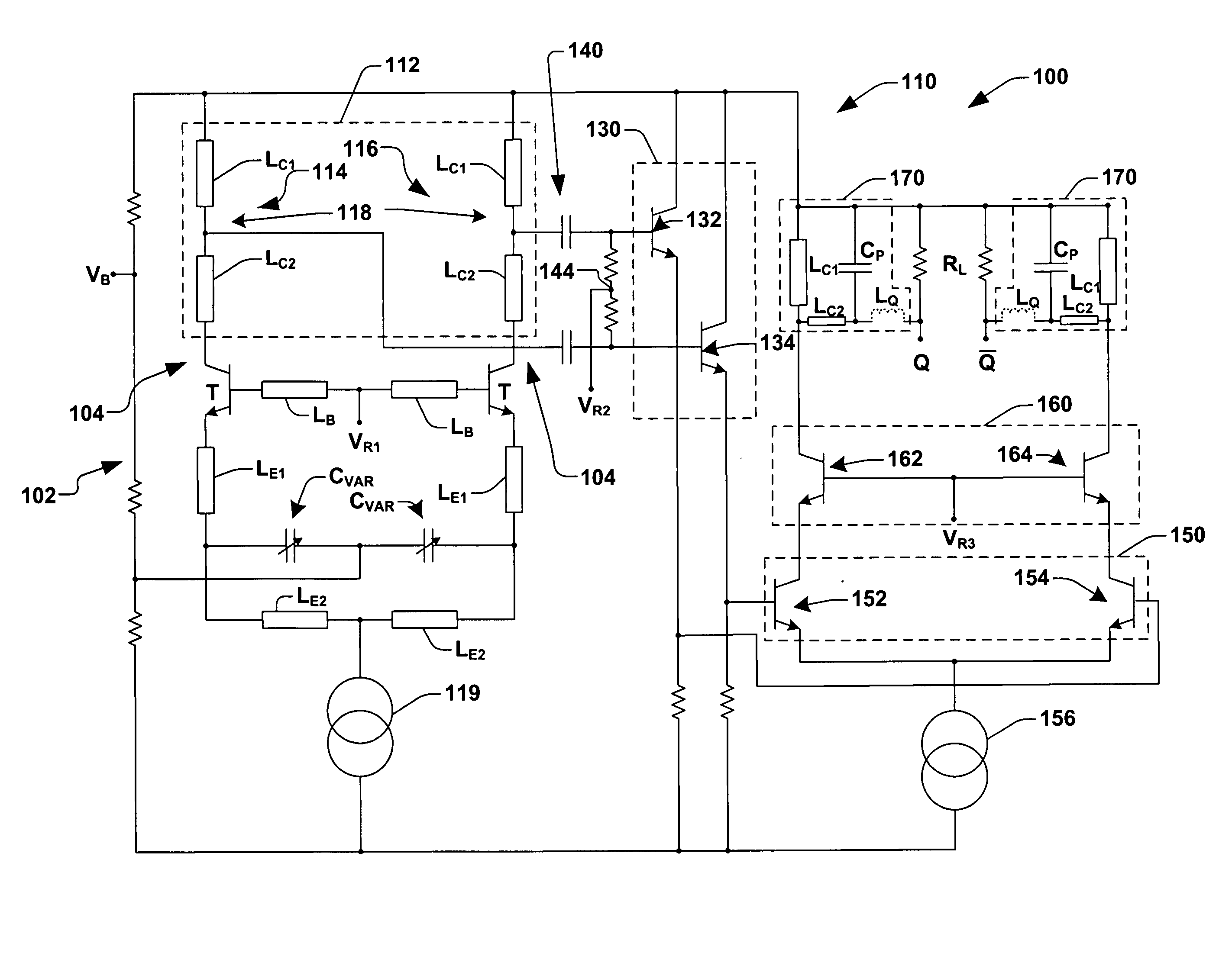
[0030] One or more implementations of the present invention will now be described with reference to the attached drawings, wherein like reference numerals are used to refer to like elements throughout. The invention relates to an oscillator system having an oscillator circuit and an output buffer. The output buffer operates in conjunction with the oscillator circuit to decouple the oscillator from an external load while providing high output power, optimization between signal amplitude and decreased loading (for improved quality factor), thus reducing phase noise.

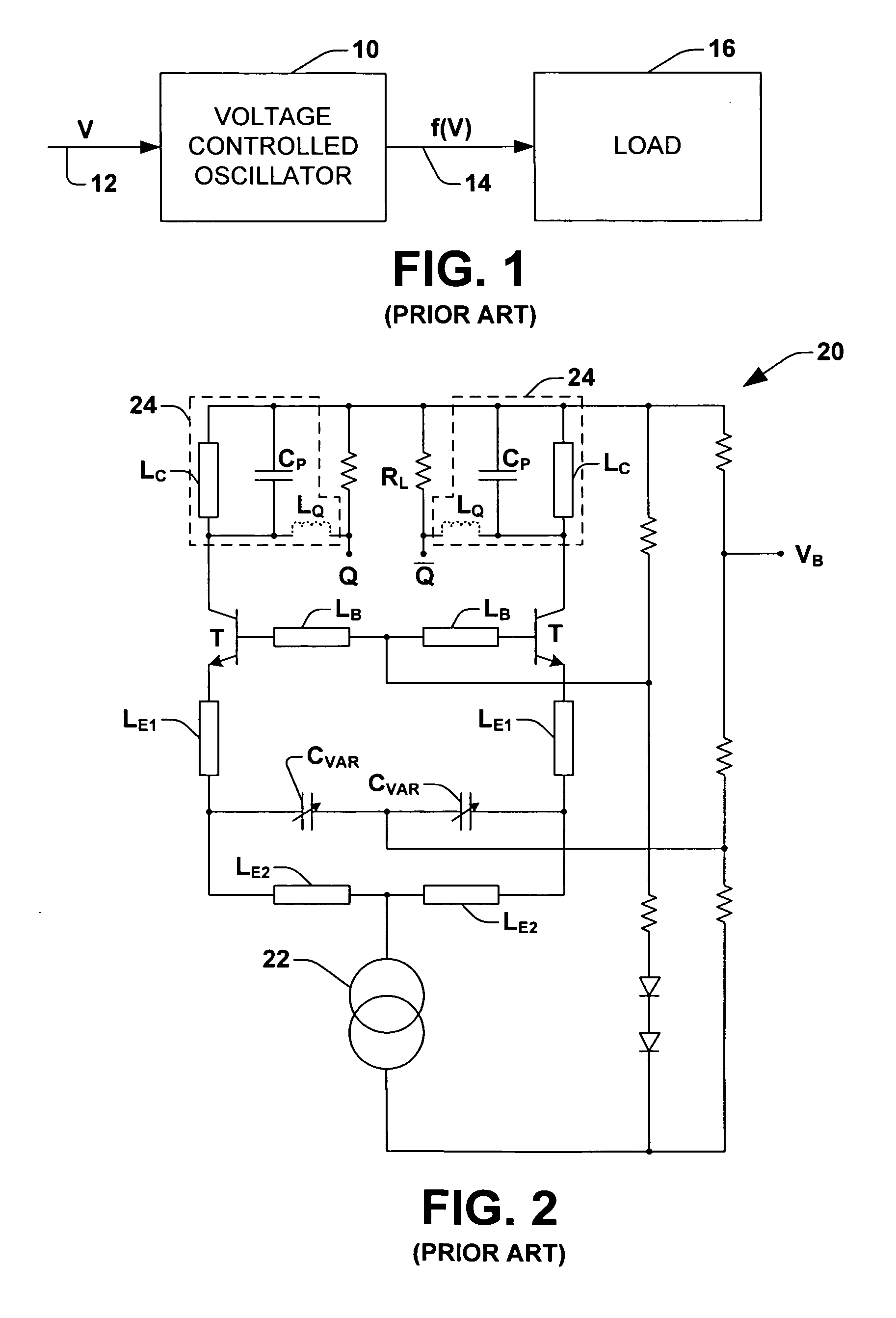
[0031] The oscillator system of the present invention is illustrated in FIG. 4, and designated at reference numeral 100. The system 100 includes an oscillator circuit 102 having a differential signal output at 104. The oscillator circuit 102 of the present example is similar to the oscillator circuit 20 of prior art FIG. 2, however, any type oscillator circuit may be employed and is contemplated as falling within the scope...


PUM


Abstract

An output buffer is disclosed and includes a differential output buffer input configured for coupling to a differential output of an input circuit. The output buffer further includes an inductive voltage divider circuit coupled to the differential output buffer input, and configured to weaken a loading at the differential output of the input circuit.

Description

REFERENCE TO RELATED APPLICATIONS [0001] This application is related to U.S. application Ser. Nos. ______ (Attorney Dockets Nos. 2004P53442US and 2004P53444US), which were both filed on Sep. 3, 2004, the entirety of which are hereby incorporated by reference.FIELD OF INVENTION [0002] The present invention relates generally to an output buffer for use in communications or sensor applications for providing effective decoupling between a circuit coupled thereto and an external load. BACKGROUND OF THE INVENTION [0003] Voltage controlled oscillators (VCOs) are generally used in high-frequency communication or sensor systems, for example, as an oscillator for a frequency synthesizer or a modulator within a wireless communication apparatus. As illustrated in prior art FIG. 1, a voltage controlled oscillator 10 receives an input or tuning voltage 12 and outputs a signal 14 having a frequency that is a function of the input voltage 12 to a load 16. Consequently, by altering the voltage at th...

Claims


Application Information

Patent Timeline
Patent Type & Authority Applications(United States)
IPC IPC(8): H03B1/00
CPCH03B5/1847H03F2203/45554H03F3/4508
Inventor REIN, HANS-MARTINLI, HAO
Owner INFINEON TECH AG
Why Eureka
Try Eureka