
Method for forming metal chalcogenide thin films on a semiconductor device

a technology of metal chalcogenide and semiconductor devices, applied in the direction of semiconductor/solid-state device details, coatings, chemical vapor deposition coatings, etc., can solve the problem of unsatisfactory increases in contact resistan

Active Publication Date: 2016-12-22
ASM IP HLDG BV
View PDF9 Cites 314 Cited by
  • Summary
  • Abstract
  • Description
  • Claims
  • Application Information

AI Technical Summary

Benefits of technology

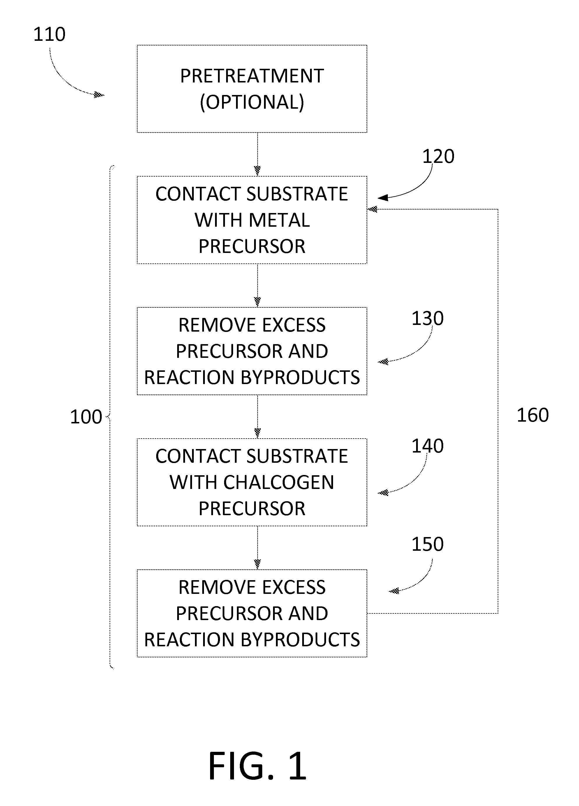
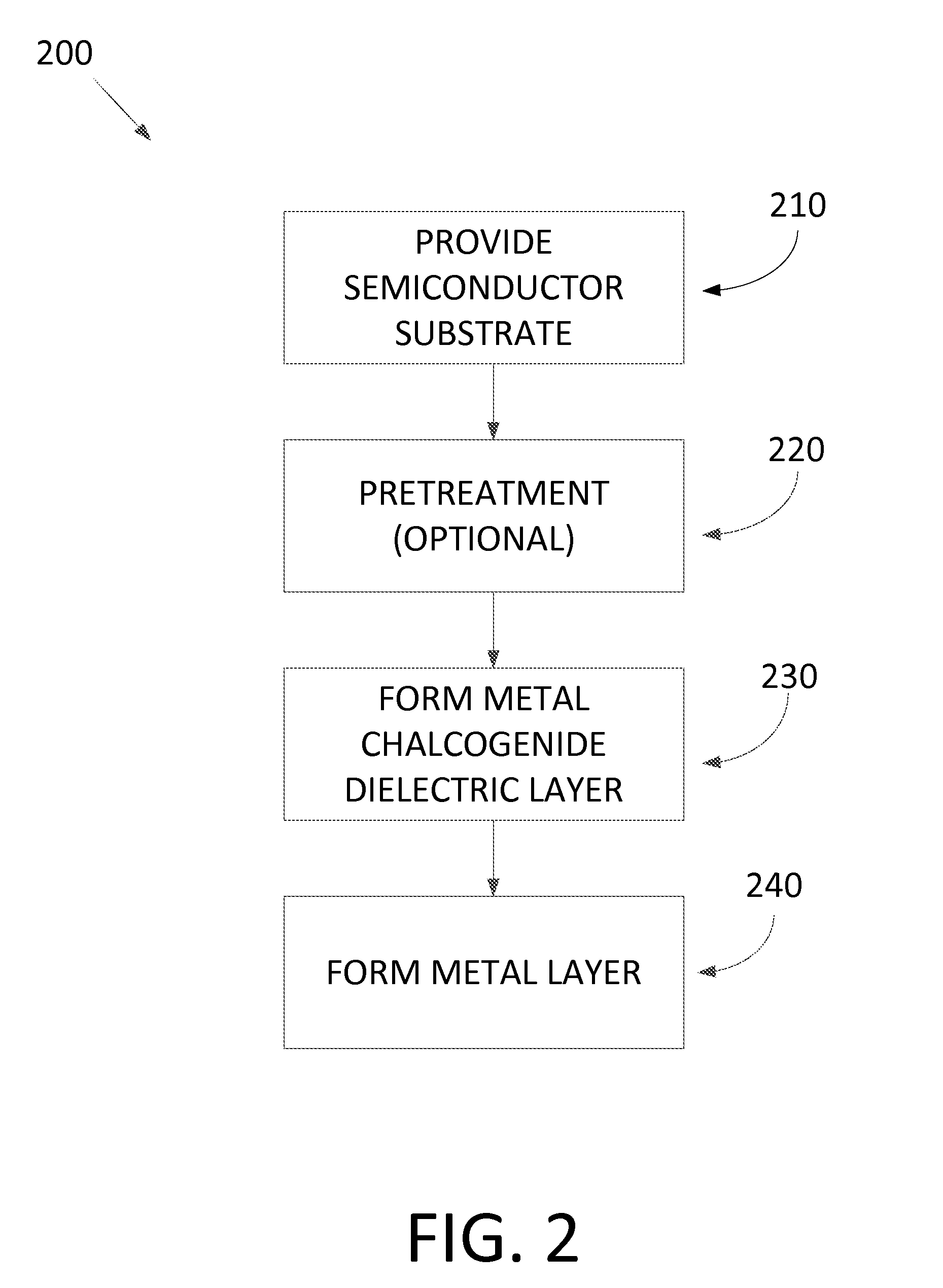
The patent text describes methods for forming metal chalcogenide thin films on a substrate surface using a cyclical process. The methods involve alternately and sequentially contacting the substrate surface with a metal precursor and a chalcogen precursor. The resulting metal chalcogenide thin film can be used to form a metal-insulator-semiconductor (MIS) structure on the substrate surface. The methods can provide a cost-effective and efficient way to deposit metal chalcogenide films with good quality and control over the deposition process. The methods can be used to form MIS structures on a variety of substrate surfaces, such as silicon, silicon germanium, or a combination of semiconductor materials.

Problems solved by technology

Smaller contact areas, however, can cause undesirable increases in contact resistance.

Method used


Image

  • Method for forming metal chalcogenide thin films on a semiconductor device
  • Method for forming metal chalcogenide thin films on a semiconductor device
  • Method for forming metal chalcogenide thin films on a semiconductor device

Examples


example 1

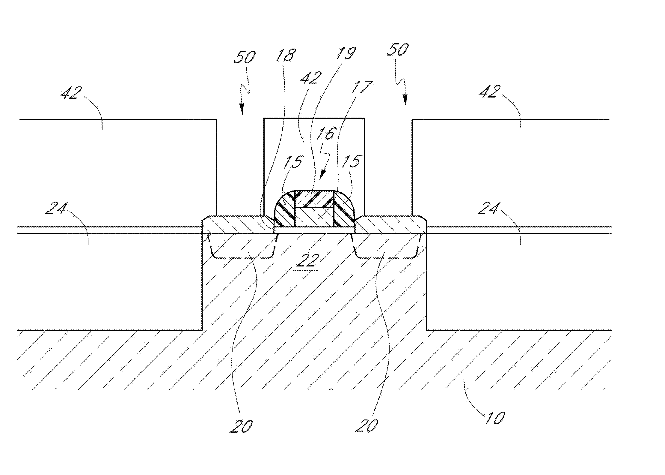
[0169]In this example, a number of metal-insulator-semiconductor (MIS) structures were formed with insulator-semiconductor interfacial layers of various compositions, and the respective Schottky barrier height (SBH) of each structure was measured.

[0170]Each MIS structure was formed with an aluminum metal layer, a TiO2 dielectric, or insulator layer, and an n-type Ge semiconductor layer. Interfacial layers of varying compositions were deposited between the n-type Ge layer and the TiO2 layer. In two separate samples, Mg(Cp)2 and Sr(Cp)2 were pulsed through a reaction space in an ALD process with a pulse time of about 30 seconds respectively without a chalcogen precursor. In two other separate samples, H2S was chosen as a chalcogen precursor. In one sample Mg(Cp)2 and the chalcogen precursor were alternately and sequentially pulsed through a reaction space in an ALD process with a metal precursor pulse times of about 30 seconds and a H2S pulse time of about 0.1 seconds to about 10 seco...

example 2

[0172]In this example, a number of metal-insulator-semiconductor (MIS) structures were formed with insulator-semiconductor interfacial layers of various compositions, and the respective Schottky barrier height (SBH) of each structure was measured.

[0173]Each MIS structure was formed with an aluminum metal layer, a TiO2 dielectric, or insulator layer, and an n-type Ge semiconductor layer. Interfacial layers of varying compositions were deposited between the n-type Ge layer and the TiO2 layer. In one sample Mg(Cp)2 was chosen as the metal precursor and H2S was chosen as the chalcogen precursor. The metal precursor was pulsed through a reaction space with a pulse time of about 3 seconds and a purge time of about 3 seconds, and the chalcogen precursor was pulsed through a reaction space with a pulse time of about 3 seconds and a purge time of about 6 seconds in an ALD process, which was carried out at about 250° C. In another sample, Mg(Cp)2 was pulsed through a reaction space with a pul...


PUM

PropertyMeasurementUnit
Thicknessaaaaaaaaaa
Thicknessaaaaaaaaaa
Semiconductor propertiesaaaaaaaaaa

Abstract

In some aspects, methods of forming a metal chalcogenide thin film are provided. According to some methods, a metal chalcogenide thin film is deposited on a substrate in a reaction space in a cyclical deposition process where at least one cycle includes alternately and sequentially contacting the substrate with a first vapor-phase metal reactant and a second vapor-phase chalcogen reactant. In some aspects, methods of forming three-dimensional structure on a substrate surface are provided. In some embodiments, the method includes forming a metal chalcogenide dielectric layer between a substrate and a conductive layer. In some embodiments the method includes forming an MIS-type contact structure including a metal chalcogenide dielectric layer.

Description

BACKGROUND OF THE INVENTION[0001]Field of the Invention[0002]The invention relates generally to the field of semiconductor device manufacturing and, more particularly, to metal chalcogenide thin films and methods for forming the same, such as by atomic layer deposition (“ALD”) processes. For example, metal chalcogenide thin films may be formed by ALD processes and may serve as a dielectric layer in a metal-insulator-semiconductor (MIS) structure.[0003]Description of the Related Art[0004]As the dimensions of semiconductor devices in integrated circuits become ever smaller, the sizes of the constituent parts of these devices are also becoming smaller. For example, the sizes of transistors are continually decreasing, leading to decreases in the sizes of transistor source / drain regions. These smaller source / drain regions provide a smaller contact area for the source / drain contacts that electrically connect the source / drain regions to other electrical features. Smaller contact areas, how...

Claims


Application Information

Patent Timeline
IPC IPC(8): H01L21/768H01L21/02
CPCH01L21/76829H01L21/02271H01L21/76895H01L21/02175H01L21/02186H01L21/0228H01L21/02304C23C16/02C23C16/045C23C16/305C23C16/45553H01L21/285H01L23/485H01L29/42364H01L29/517H01L21/76814H01L29/78H01L21/76831H01L21/76843H01L21/02485H01L21/02568H01L21/28194H01L21/28556
Inventor TANG, FUGIVENS, MICHAEL EUGENEWOODRUFF, JACOB HUFFMANXIE, QIMAES, JAN WILLEM
Owner ASM IP HLDG BV
Learn More