LOW PARASITIC CAPACITANCE AND RESISTANCE finFET DEVICE

a capacitance and resistance finfet technology, applied in the field of low parasitic capacitance and resistance finfet devices, can solve the problems of short circuits, defective devices, and encroachment of nickel silicides

Inactive Publication Date: 2016-12-22
IBM CORP
View PDF11 Cites 5 Cited by
  • Summary
  • Abstract
  • Description
  • Claims
  • Application Information

AI Technical Summary

Benefits of technology

This patent describes a semiconductor structure with raised active regions on semiconductor fins. These active regions have angled sidewall surfaces and are made of silicon germanium. The structure also includes a metal semiconductor alloy region that contacts the angled sidewall surfaces of adjacent raised active regions. The technical effects include improved performance of semiconductor devices and increased efficiency of semiconductor chips. Additionally, the disclosed method provides a way to form the semiconductor structure efficiently.

Problems solved by technology

Another yield challenge with finFET devices is nickel silicide encroachment.
If over-etching occurs nickel can encroach on silicon fins which results in short circuits and defective devices.

Method used


Image

  • LOW PARASITIC CAPACITANCE AND RESISTANCE finFET DEVICE
  • LOW PARASITIC CAPACITANCE AND RESISTANCE finFET DEVICE
  • LOW PARASITIC CAPACITANCE AND RESISTANCE finFET DEVICE

Examples


Embodiment Construction

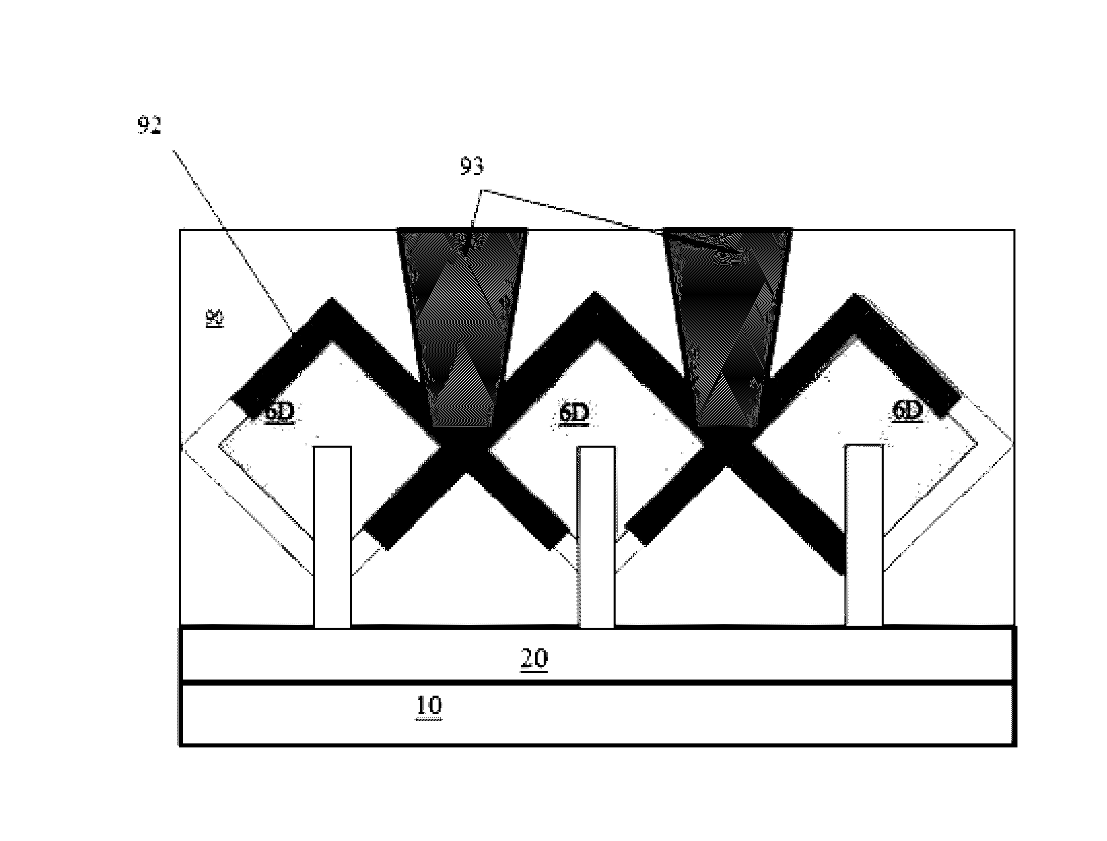
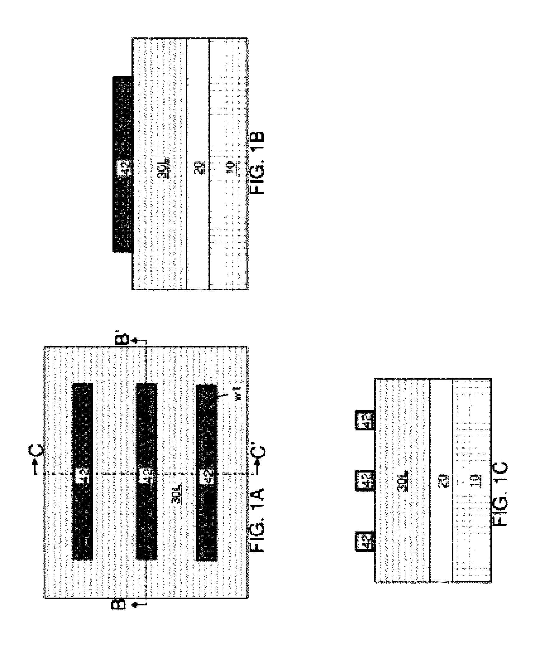
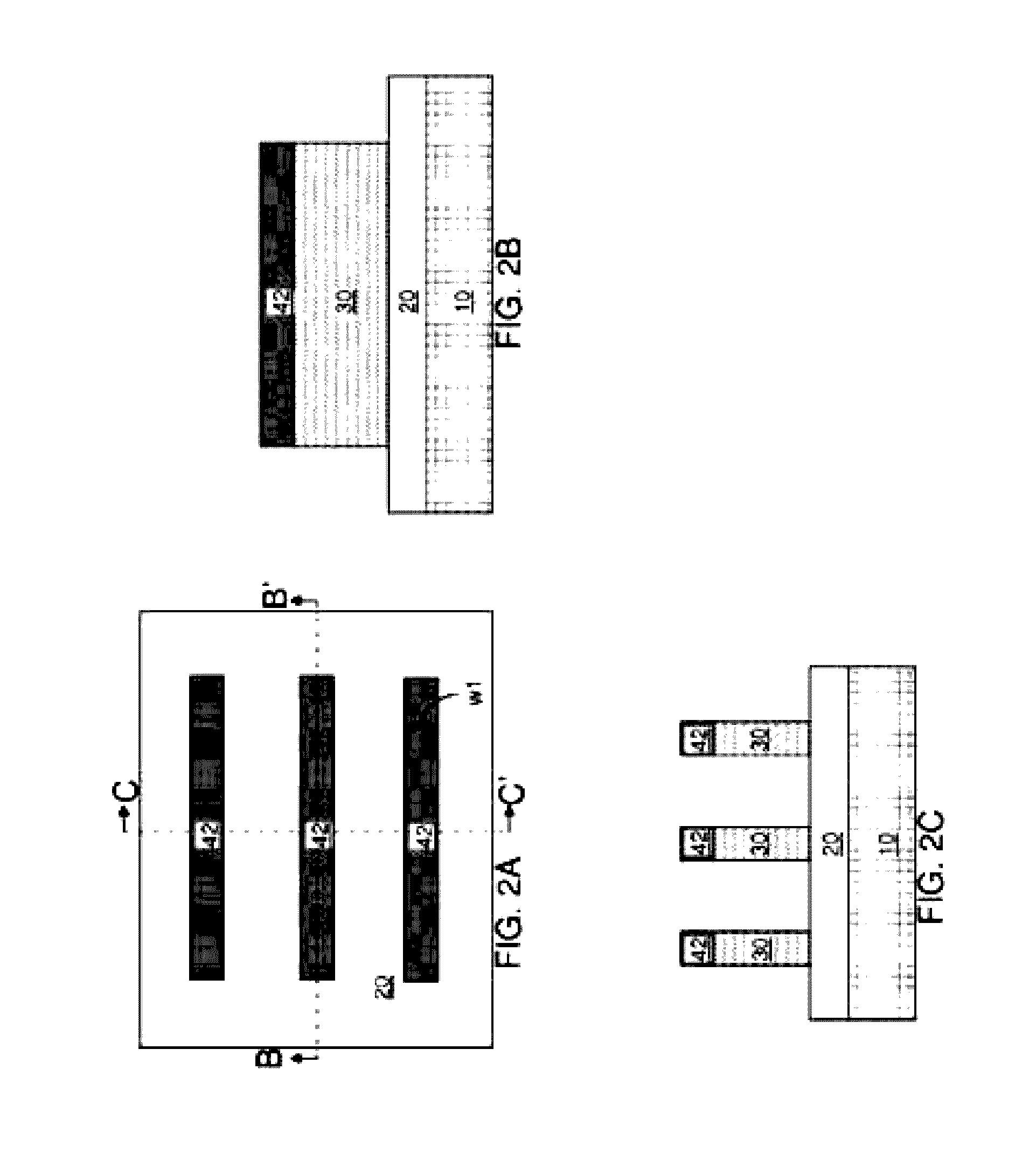
[0033]As stated above, the present disclosure relates to fin field effect transistors (finFETs) and a method of manufacturing the same. Aspects of the present disclosure are now described in detail with accompanying figures. It is noted that like reference numerals refer to like elements across different embodiments. The drawings are not necessarily drawn to scale.

[0034]Referring to FIGS. 1A-1C, an exemplary semiconductor structure according to the present disclosure includes a vertical stack of a substrate 10, and an insulator layer 20, and a semiconductor layer 30L.

[0035]The substrate 10 can include a semiconductor material, an insulator material, or a conductive material. The substrate 10 provides mechanical support to the insulator layer 20 and the semiconductor layer 30L. The substrate 10 can be single crystalline, polycrystalline, or amorphous. The thickness of the substrate 10 can be from 50 microns to 2 mm, although lesser and greater thicknesses can also be employed.

[0036]T...


PUM


Abstract

Described herein is a semiconductor structure and method of manufacture. The semiconductor structure includes a plurality of semiconductor fins on a substrate and a plurality of raised active regions, wherein each raised active region is located on sidewalls of a corresponding semiconductor fin among said plurality of semiconductor fins. The raised active regions are laterally spaced from any other of the raised active regions. Each raised active region comprises angled sidewall surfaces that are not parallel or perpendicular to a topmost horizontal surface of said substrate. The raised active regions are silicon germanium (SiGe). The semiconductor structure includes a metal semiconductor alloy region contacting at least said angled sidewall surfaces of at least two adjacent raised active regions. The semiconductor alloy region includes a material selected from the group consisting of nickel silicide, nickel-platinum silicide and cobalt silicide.

Description

FIELD OF INVENTION[0001]The present disclosure relates to a semiconductor structure, and particularly to fin field effect transistors including metal semiconductor alloy portions, and a method of manufacturing the same.BACKGROUND[0002]State-of-the art complementary metal oxide semiconductor (CMOS) devices employ fin field effect transistors (finFET). One of the design choices is whether raised active regions formed by selective epitaxy are to be merged with one another or remain unmerged. Each choice offers advantages and disadvantages. On one hand, fin field effect transistors including unmerged raised active regions benefit from lower contact resistance and improved direct current (DC) performance due to increased silicide contact areas corresponding to wrapping around of the silicides around the faceted surfaces of the unmerged raised active regions. On the other hand, fin field effect transistors including merged raised active regions benefit from reduced parasitic capacitance b...

Claims


Application Information

Patent Timeline
Patent Type & Authority Applications(United States)
IPC IPC(8): H01L29/78H01L29/08H01L29/66H01L29/161
CPCH01L29/7845H01L29/785H01L29/665H01L29/0847H01L29/66795H01L29/161H01L29/165H01L29/41791
Inventor GLUSCHENKOV, OLEGOZCAN, AHMET S.
Owner IBM CORP
Why Eureka
Try Eureka