Element

a technology of elements and elements, applied in the field of elements, can solve the problems of difficult circuit arrangement, difficult to employ the method of oscillator employing a microstrip resonator, and usually generate parasitic oscillation of oscillators using negative resistance elements

Active Publication Date: 2016-12-29
CANON KK
View PDF1 Cites 1 Cited by
  • Summary
  • Abstract
  • Description
  • Claims
  • Application Information

AI Technical Summary

Benefits of technology

[0010]The present invention provides an element which oscillates or detects terahertz waves and which includes a resonance unit including a differential negative resistance element, a first conductor, a second conductor, and a dielectric body, a bias circuit configured to supply a bias voltage to the differential negative resistance element, and a line configured to connect the resonance unit and the bia...

Problems solved by technology

Oscillators using a negative resistance element usually generate parasitic oscillation caused by a bias circuit which includes a power source and wiring which are used to control a bias voltage of the negative resistance element.
The method employed in NPL 1 is employed only for slot...

Method used


Image

  • Element
  • Element
  • Element

Examples


first example

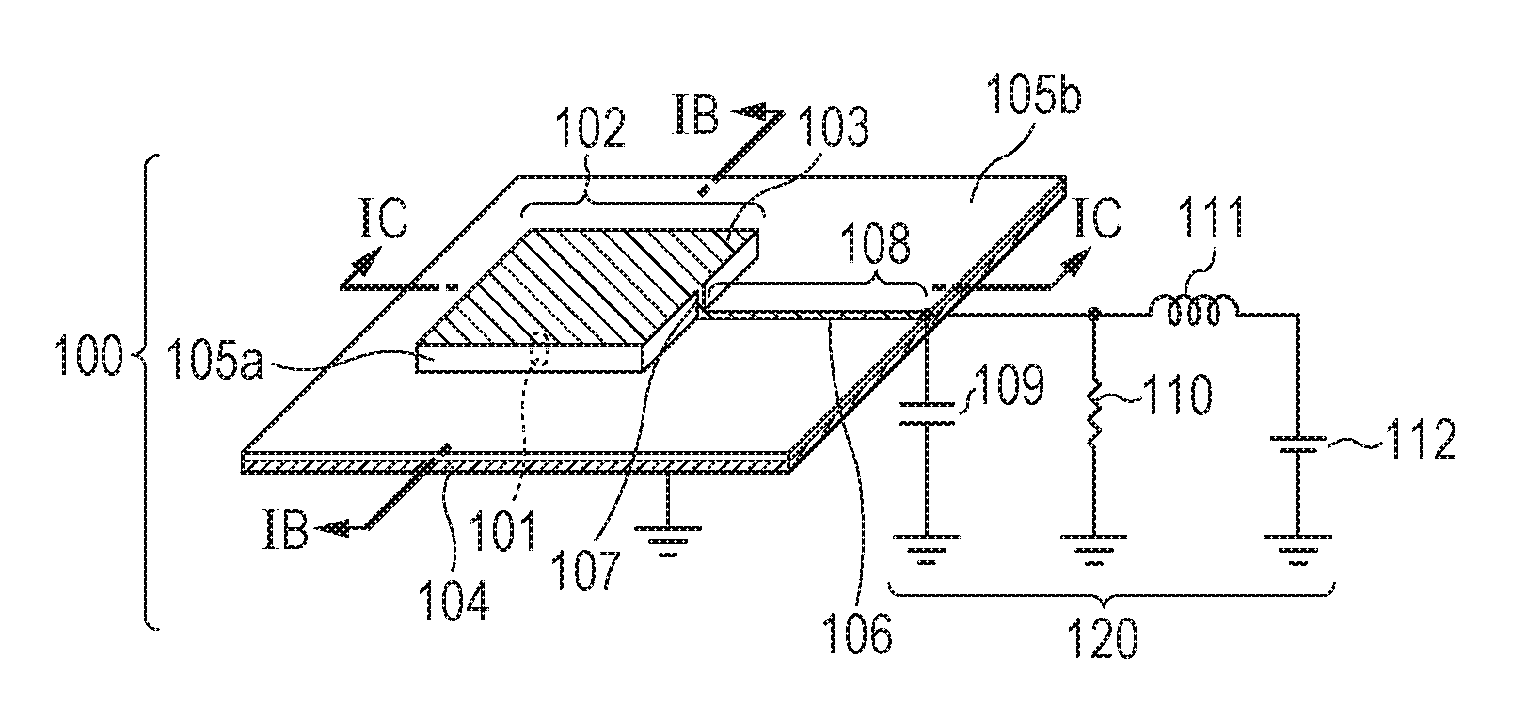
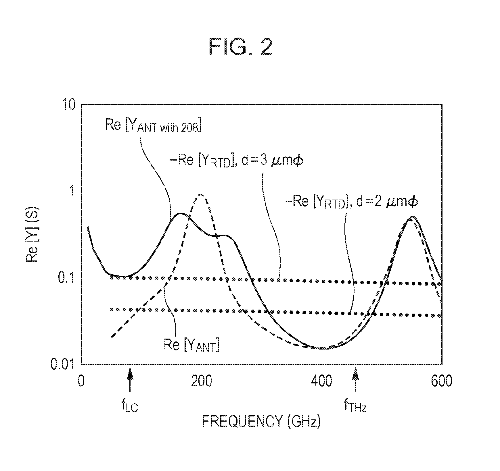
[0080]A configuration of the oscillator 200 which is an element oscillating terahertz waves of this example will be described. FIG. 3A is a perspective view of the oscillator 200. The oscillator 200 is an element which oscillates an oscillation frequency fTHz of 0.45 THz. In this example, a resonant tunneling diode (RTD) is used as the differential negative resistance element 201. The RTD 201 of this example has a multiple quantum well structure of InGaAs / InAlAs and InGaAs / AlAs on an InP substrate 230 and an electrical contact layer formed by n-InGaAs.

[0081]As the multiple quantum well structure, a triple-barrier structure is used. Specifically, a semiconductor multiple layer structure is configured by AlAs (approximately 1.3 nm) / InGaAs (approximately 7.6 nm) / InAlAs (approximately 2.6 nm) / InGaAs (approximately 5.6 nm) / AlAs (approximately 1.3 nm). In this structure, InGaAs corresponds to a well layer and lattice matching InAlAs and lattice mismatching AlAs correspond to a barrier lay...

second example

[0102]In a second example, elements of first to third modifications of the oscillator 200 according to the first example will be described. First, a structure of an oscillator 300 serving as an element of the first modification will be described with reference to FIGS. 4A and 4B. FIG. 4A is a perspective view of the element 300, and FIG. 4B is a sectional view of the element 300 taken along a line IVB-IVB of FIG. 4A. As with the oscillator 200, the oscillator 300 is an element which oscillates an oscillation frequency fTHz of 0.45 THz. A structure of a resonance unit 302 of the oscillator 300 is different from that of the resonance unit 202 of the oscillator 200. Furthermore, a structure of a line 308 of the oscillator 300 is also different from that of the line 208 of the oscillator 200 according to the first example. The structure of the line is designed where appropriate. Other configurations are the same as those of the oscillator 200, and detailed descriptions thereof are omitt...


PUM


Abstract

An element which oscillates or detects terahertz waves includes a resonance unit including a differential negative resistance element, a first conductor, a second conductor, and a dielectric body, a bias circuit configured to supply a bias voltage to the differential negative resistance element, and a line configured to connect the resonance unit and the bias circuit to each other. The differential negative resistance element and the dielectric body are disposed between the first and second conductors. The line is a low impedance line in a frequency fLC of resonance caused by inductance of the line and capacitance of the resonance unit using an absolute value of a differential negative resistance of the differential negative resistance element as a reference.

Description

TECHNICAL FIELD[0001]The present invention relates to an element which oscillates or detects terahertz waves.BACKGROUND ART[0002]Oscillators including a resonator integrated in a negative resistance element have been widely used as current injection light sources which generate electromagnetic waves (hereinafter referred to as “terahertz waves”) in a frequency domain from a millimeter waveband to a terahertz waveband (from 30 GHz inclusive to 30 THz inclusive). PTL 1 discloses an oscillator for terahertz waves which includes a double barrier resonant tunneling diode (hereinafter simply referred to as an “RTD” where appropriate) serving as a negative resistance element and a micro-strip resonator which are integrated in the same substrate.[0003]Oscillators using a negative resistance element usually generate parasitic oscillation caused by a bias circuit which includes a power source and wiring which are used to control a bias voltage of the negative resistance element. The parasitic...

Claims


Application Information

Patent Timeline
IPC IPC(8): H03B7/08H03H11/52H03B9/12
CPCH03B7/08H03B2009/123H03H11/52H03B9/12H03H7/0123
Inventor KOYAMA, YASUSHI
Owner CANON KK
Why Eureka
Try Eureka