

Invisible light flat plate detector and manufacturing method thereof, imaging apparatus
a technology of flat plate detector and manufacturing method, applied in the field of detection technology, can solve problems such as affecting detection precision, and achieve the effects of improving performance, small volume, and convenient realization
- Summary
- Abstract
- Description
- Claims
- Application Information
AI Technical Summary
Benefits of technology
Problems solved by technology
Method used
Image

Examples
first embodiment
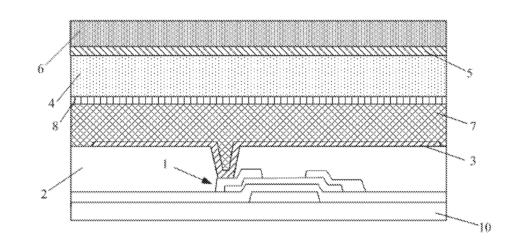
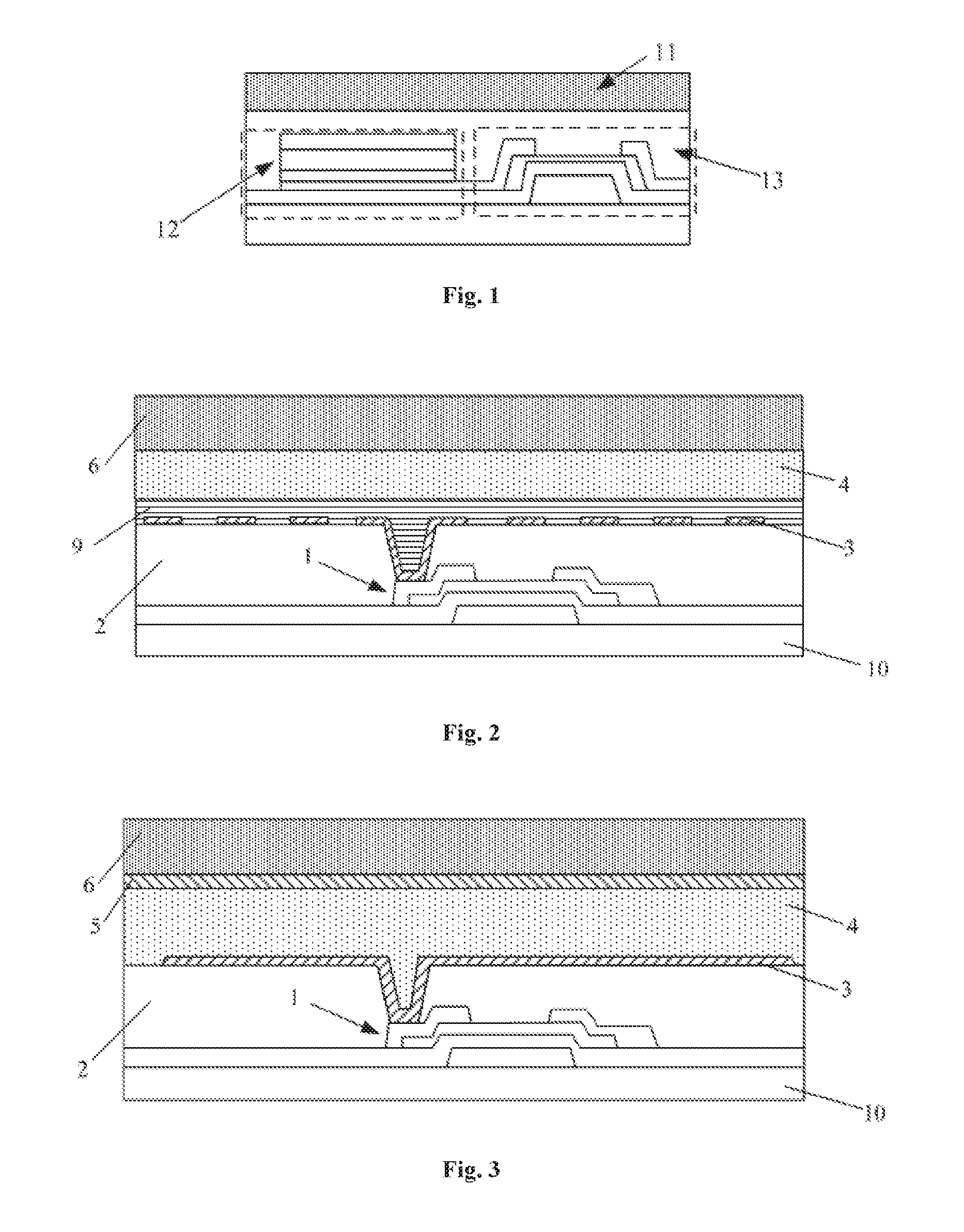
[0046]FIG. 3 is a schematic diagram showing an X-ray flat plate detector in the first embodiment of the present invention. As shown in FIG. 3, the present embodiment provides an X-ray flat plate detector, comprising a plurality of detection units provided on a substrate 10, and an invisible light conversion layer 6 provided above the detection units, each of the detection units comprising a thin film transistor 1, and a first insulation layer 2, a first electrode 3 (sensing / receiving electrode), a semiconductor photoelectronic conversion module 4 (which at least comprises a semiconductor photoelectronic conversion layer 41 as shown in FIGS. 5-6), a second electrode 5 which are successively provided on the substrate 10, and projections of the first insulation layer 2, the first electrode 3, the semiconductor photoelectronic conversion module 4, the second electrode 5 on the substrate 10 at least partially overlap with a projection of the thin film transistor 1 on the substrate 10.
[00...
second embodiment
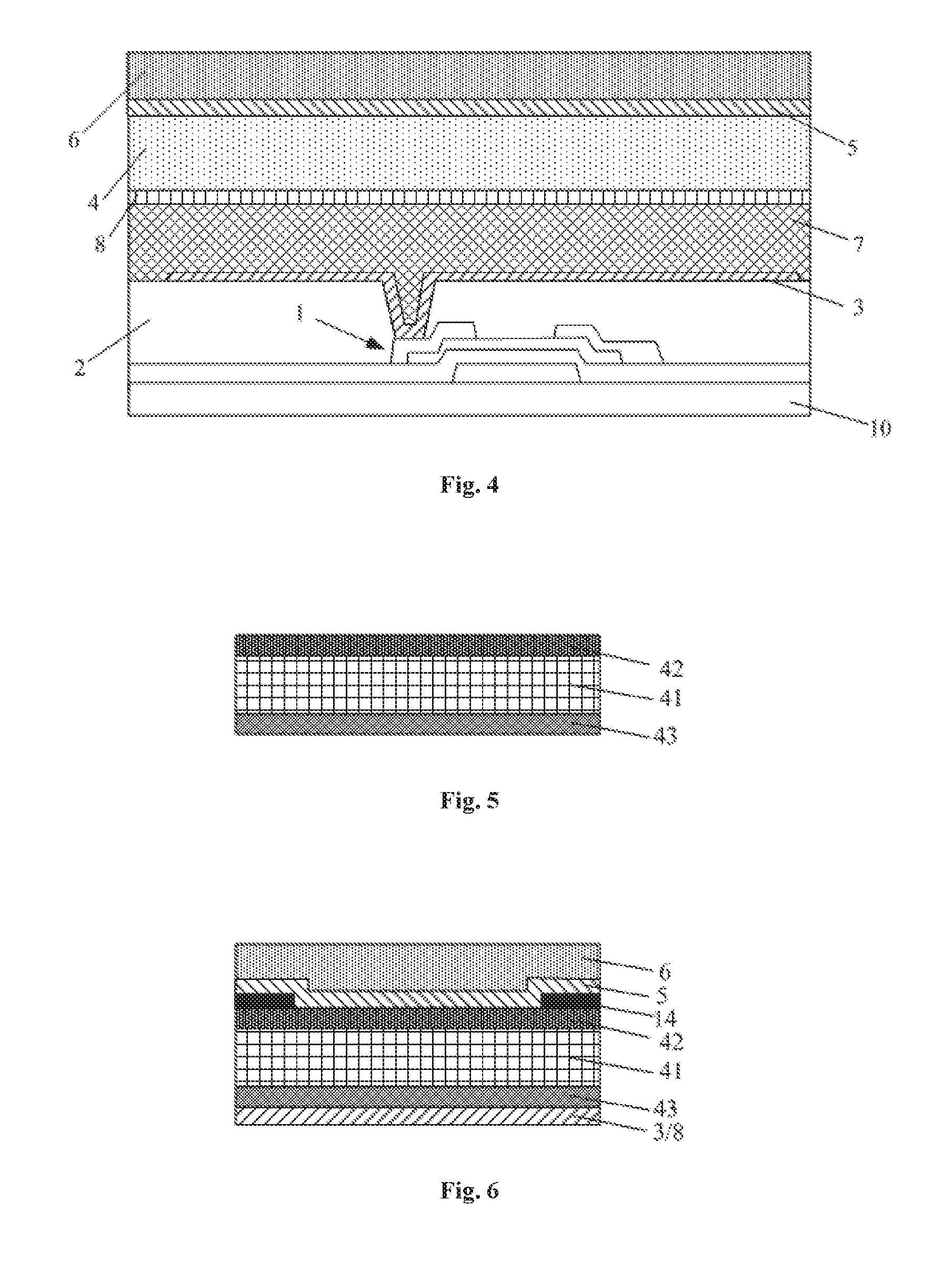
[0069]FIG. 4 is a schematic diagram showing an X-ray flat plate detector in the second embodiment of the present invention. As shown in FIG. 4, the present embodiment provides an X-ray flat plate detector, comprising a plurality of detection units provided on a substrate 10, and an X-ray conversion layer 6 provided above the detection units, wherein, each of the detection units comprising a thin film transistor 1, and a first insulation layer 2, a first electrode 3 (sensing electrode), a second insulation layer 7, a third electrode 8 (receiving electrode), a semiconductor photoelectronic conversion module 4 (which at least comprises a semiconductor photoelectronic conversion layer 41 as shown in FIGS. 5-6), a second electrode 5 which are successively provided on the substrate 10, and projections of the first insulation layer 2, the first electrode 3, the second insulation layer 7, the third electrode 8, the semiconductor photoelectronic conversion module 4, the second electrode 5 on...
third embodiment
[0095]The present embodiment provides an imaging apparatus. The imaging apparatus may comprise the X-ray flat plate detector of the first or second embodiment. The imaging apparatus may be any product or component having displaying function, such as a liquid crystal panel, an electronic paper, an OLED panel, a mobile phone, a tablet computer, a display device, a notebook computer or the like.
[0096]Of course, when the invisible light is from other light source such as an infrared ray source, an ultraviolet ray source or the like, the imaging apparatus also may correspondingly comprise an infrared ray flat plate detector, an ultraviolet ray flat plate detector or the like.
PUM
| Property | Measurement | Unit |
|---|---|---|
| thickness | aaaaa | aaaaa |
| semiconductor | aaaaa | aaaaa |
| conductive | aaaaa | aaaaa |
Abstract
Description
Claims
Application Information