Method of fabricating semiconductor device

a semiconductor device and fabrication method technology, applied in the direction of semiconductor devices, diodes, radiation controlled devices, etc., can solve the problems of current leakage of semiconductor devices, deterioration of image quality, and generation of more read-out noises, so as to achieve effective rectifying lattice defects

Inactive Publication Date: 2017-01-12
POWERCHIP TECH CORP
View PDF4 Cites 0 Cited by
  • Summary
  • Abstract
  • Description
  • Claims
  • Application Information

AI Technical Summary

Benefits of technology

[0005]The invention is directed to a method of fabricating a semiconductor device for effectively rectifying lattice defects.

Problems solved by technology

Generally, as to fabrication of semiconductor devices, manufacturing defects often arise in the substrates, such as damages to sidewalls of shallow trench isolation (STI) structures, lattice defects including stacking fault or lattice dislocation caused by ion implantation, and so on, which often leads to current leakage of the semiconductor devices.
For instance, if the lattice defects including stacking fault or lattice dislocation exist in a complementary metal oxide semiconductor (CMOS) image sensor (CIS), the issue of dark current occurs, such that more read-out noises are generated, and that the image quality may be deteriorated.

Method used


Image

  • Method of fabricating semiconductor device
  • Method of fabricating semiconductor device
  • Method of fabricating semiconductor device

Examples


Embodiment Construction

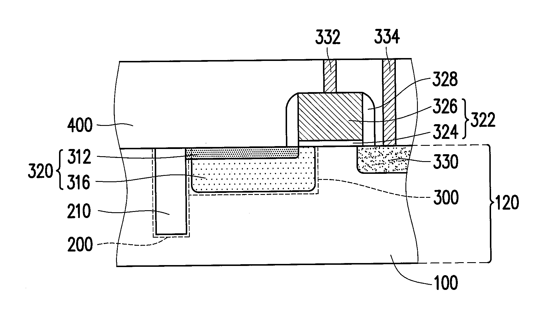
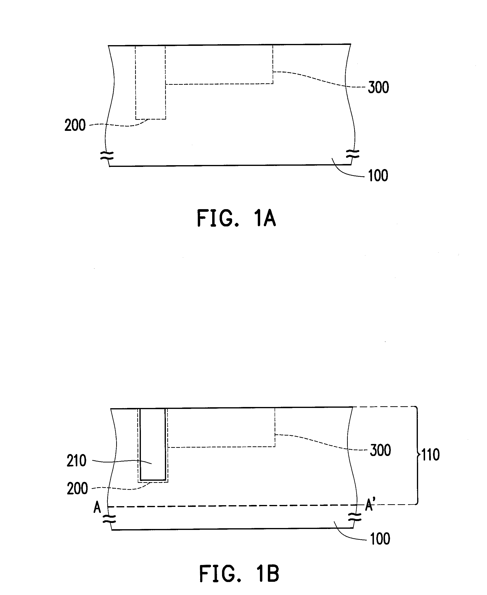
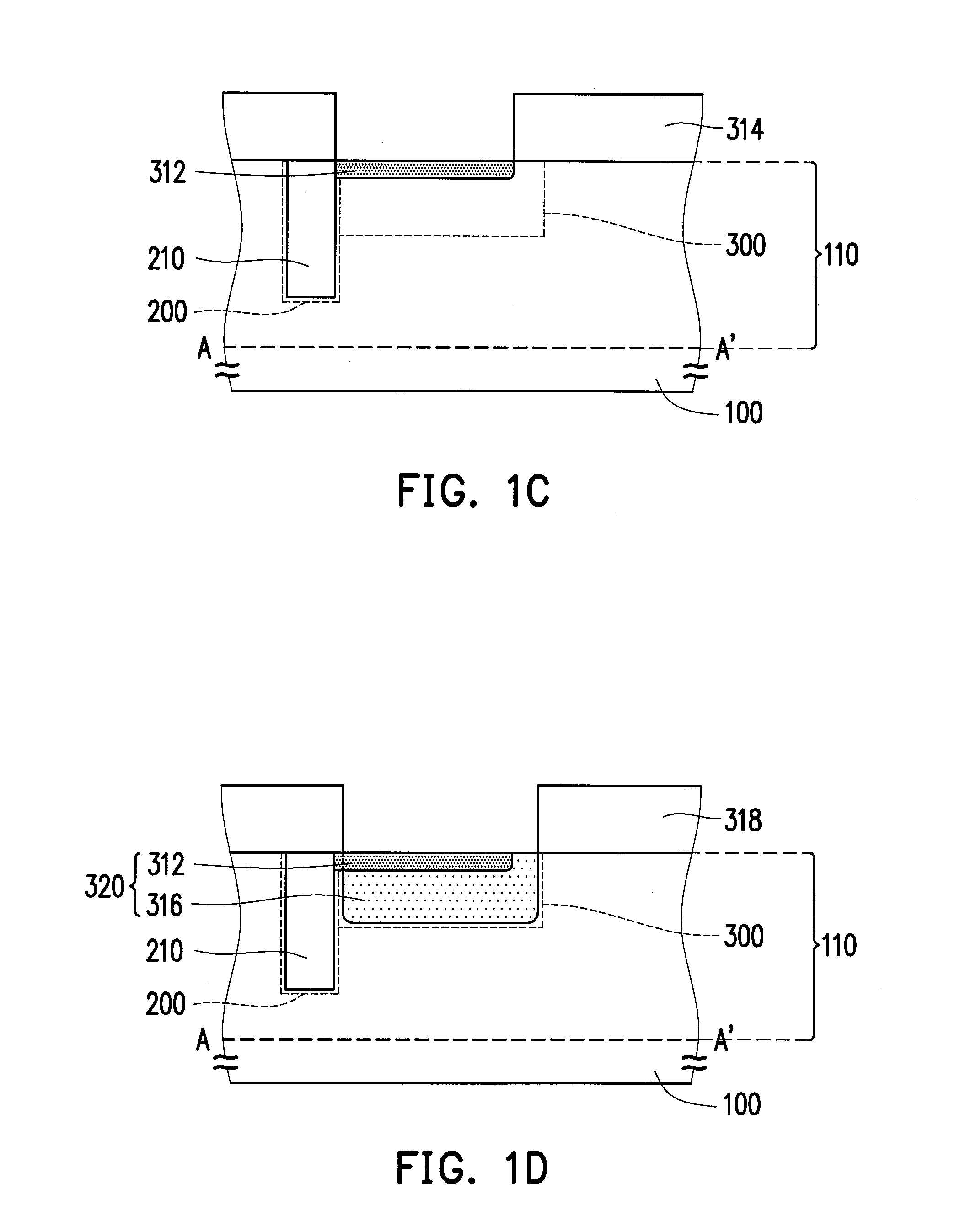
[0031]FIG. 1A to FIG. 1F are cross-sectional views illustrating a method of manufacturing a semiconductor device according to an embodiment of the invention.

[0032]With reference to FIG. 1A, a substrate 100 is provided. The substrate 100 is, for example, a silicon substrate. P-type dopants or an n-type dopants may be implanted into the substrate 100 to form a p-type substrate or an n-type substrate. According to the present embodiment, the substrate 100 is, for instance, the p-type substrate.

[0033]The substrate 100 includes an isolation region 200 and a device region 300. An isolation structure is to be formed in the isolation region 200, and the semiconductor device is to be formed in the device region 300.

[0034]With reference to FIG. 1B, an isolation structure 210 can be formed in the isolation region 200. The isolation structure 210 is a shallow trench isolation (STI) structure, a deep trench isolation (DTI) structure, or a junction isolation structure, for instance. In the presen...


PUM

PropertyMeasurementUnit
depthaaaaaaaaaa
temperatureaaaaaaaaaa
timeaaaaaaaaaa

Abstract

A method of fabricating a semiconductor device includes the following steps. A substrate including an isolation region and a device region is provided. An overall amorphization process is performed on the substrate to form an amorphous region. Here, a minimum depth of the amorphous region is greater than a maximum depth of at least one of the isolation region and the device region, and the amorphous region covers at least one of the isolation region and the device region. A thermal treatment is performed on the amorphous region.

Description

CROSS-REFERENCE TO RELATED APPLICATION[0001]This application claims the priority benefit of Taiwan application serial no. 104122109, filed on Jul. 8, 2015. The entirety of the above-mentioned patent application is hereby incorporated by reference herein and made a part of this specification.FIELD OF INVENTION[0002]The invention relates to a method of fabricating a semiconductor device. More particularly, the invention relates to a method of fabricating a semiconductor device for repairing lattice defects.DESCRIPTION OF RELATED ART[0003]Generally, as to fabrication of semiconductor devices, manufacturing defects often arise in the substrates, such as damages to sidewalls of shallow trench isolation (STI) structures, lattice defects including stacking fault or lattice dislocation caused by ion implantation, and so on, which often leads to current leakage of the semiconductor devices.[0004]For instance, if the lattice defects including stacking fault or lattice dislocation exist in a c...

Claims


Application Information

Patent Timeline
Patent Type & Authority Applications(United States)
IPC IPC(8): H01L27/146H01L31/20
CPCH01L27/14687H01L27/14689H01L31/208H01L21/02365H01L21/02656H01L21/02669H01L21/324H01L27/1463H01L27/14643H01L27/14692
Inventor LEE, SHIH-PINGCHEN, YU-ANHUANG, HSIU-WENCHANG, CHUAN-HUA
Owner POWERCHIP TECH CORP
Why Eureka
Try Eureka